BJT Switching Characteristics
Possible Exam Questions
Exam Questions and Answer Map
Questions marked [PYQ paper/year] were directly observed in past papers; [likely] means pattern-based prediction.
-
Explain how a BJT operates as a switch (cut-off and saturation regions) with the load line. [5] — [likely]
-
Answer plan: Define BJT switch → state cutoff and saturation conditions → draw the load line → mark OFF and ON operating points.
-
Model answer: BJT as a Switch with Load Line
-
Describe BJT turn-on, turn-off, delay, rise, storage and fall times. [5] — [likely]
-
Answer plan: Draw the switching waveform → define each interval → write \(t_{ON}=t_d+t_r\) and \(t_{OFF}=t_s+t_f\) → explain why storage time dominates.
- Model answer: BJT Switching Characteristics
1. Bipolar Junction Transistor (BJT) Switching Characteristics
Likely Exam Questions
"Explain the switching characteristics of a BJT. Define all switching time parameters with waveform." OR "Why is storage time a critical parameter in BJT switching? How can it be reduced?"
Definition
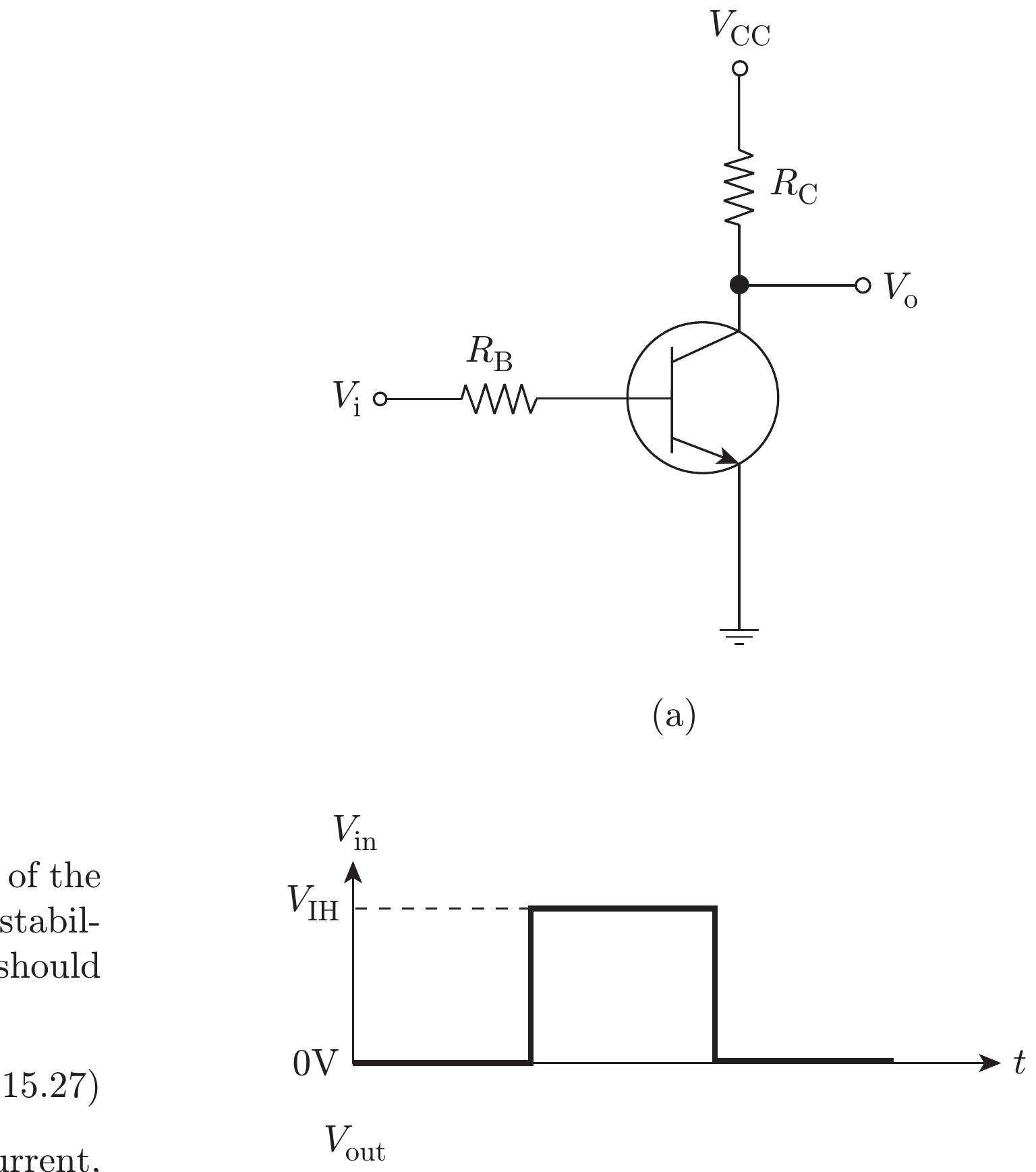
A Bipolar Junction Transistor (BJT) is a three-terminal (Base, Collector, Emitter) current-controlled semiconductor device. When used as a switch, it is driven between two extreme operating regions — cutoff (OFF state, no collector current flows) and saturation (ON state, maximum collector current flows, \(V_{CE}\) drops to a very small value \(\approx 0.2\,\text{V}\)). Unlike its use as a linear amplifier (active region), a BJT switch is intentionally forced into these two boundary states.
Regions of Operation of a BJT
| Region | Emitter-Base Junction | Collector-Base Junction | Condition | Behaviour |
|---|---|---|---|---|
| Cutoff | Reverse biased | Reverse biased | \(V_{BE} < V_\gamma \approx 0.5\,\text{V}\) | OFF state: \(I_C \approx 0\), \(V_{CE} \approx V_{CC}\) (open switch) |
| Active | Forward biased | Reverse biased | \(V_{BE} \geq 0.7\,\text{V}\), \(V_{CE} > V_{CE(sat)}\) | Linear amplification: \(I_C = \beta\, I_B\) |
| Saturation | Forward biased | Forward biased | \(V_{BE} \geq 0.7\,\text{V}\), \(V_{CE} \leq V_{CE(sat)}\) | ON state: \(V_{CE(sat)} \approx 0.2\,\text{V}\) (closed switch) |
In switching applications, the BJT operates only in cutoff and saturation; the active region is merely a transition zone.
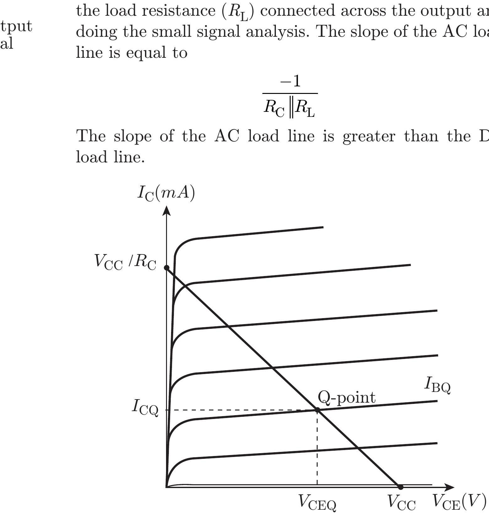
Output characteristics (\(I_C\) vs \(V_{CE}\)) for stepped \(I_B\), with the DC load line \(I_C=(V_{CC}-V_{CE})/R_C\); the switch toggles between the OFF point (cutoff) and the ON point (saturation).
Switching Time Parameters
The transition between cutoff and saturation is not instantaneous because of charge storage effects in the base region. The total switching waveform is characterised by the following time intervals:
Turn-ON Phase:
-
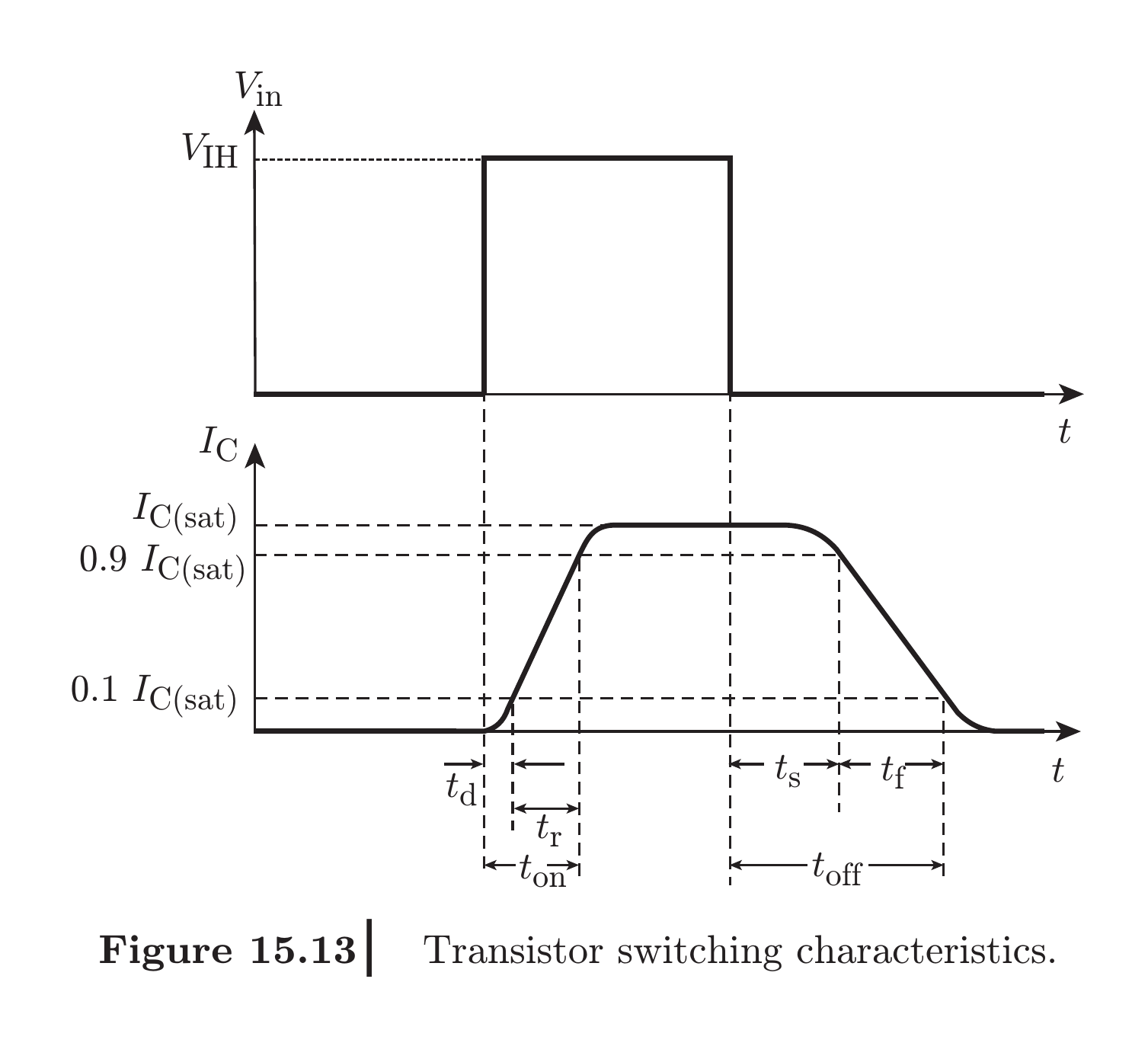
Delay time (\(t_d\)) — The time taken for the collector current \(I_C\) to rise from zero to 10% of its final saturation value after the input pulse is applied. During \(t_d\), the base-emitter junction capacitance charges up to the threshold voltage \(V_\gamma\).
-
Rise time (\(t_r\)) — The time taken for \(I_C\) to rise from 10% to 90% of its saturation value \(I_{C(sat)}\).
Turn-OFF Phase:
-
Storage time (\(t_s\)) — After the input is removed (or reversed), the collector current remains at \(I_{C(sat)}\) for a period \(t_s\) before it begins to fall. This is the most critical delay in BJT switching. During saturation, both junctions are forward biased, and excess minority carriers (electrons in the base for NPN) accumulate in the base region. These stored carriers must be swept out or recombined before the transistor can begin to turn off.
-
Fall time (\(t_f\)) — The time taken for \(I_C\) to fall from 90% to 10% of its saturation value.
Total switching time: \(t_{sw} = t_{ON} + t_{OFF} = (t_d + t_r) + (t_s + t_f)\)

Book-grounded timing checklist
- Measure \(t_d\) from the input transition to \(I_C=0.1I_{C(sat)}\) and \(t_r\) from \(0.1I_{C(sat)}\) to \(0.9I_{C(sat)}\).
- Measure \(t_s\) while collector current remains near saturation after drive removal, then \(t_f\) from 90% to 10%.
- Hence \(t_{on}=t_d+t_r\) and \(t_{off}=t_s+t_f\); the labelled thresholds belong on an exam sketch.
Source figure: Maini, Acing the GATE ECE, PDF p. 352.
Charge Storage and Storage Time
When a BJT is driven into saturation, the base receives more current than the minimum needed (\(I_{B} > I_{B(min)}\)). This causes excess charge \(Q_s\) to be stored in the base:
where \(\tau_s\) is the minority carrier lifetime in the base region.
The storage time is estimated as:
where \(I_{B(\text{forward})}\) is the forward base drive current and \(I_{B(\text{reverse})}\) is the reverse base current applied during turn-off.
The deeper the saturation (larger overdrive), the more charge is stored, and the longer it takes to turn off. This is the fundamental speed-power trade-off in BJT switching.
Techniques to Reduce Storage Time
| Technique | How It Works |
|---|---|
| Schottky clamping | A Schottky Barrier Diode (SBD) is connected across the B-C junction. Since \(V_{SBD} \approx 0.3\,\text{V} < V_{BC(fwd)} \approx 0.7\,\text{V}\), the diode clamps \(V_{BC}\) and prevents the transistor from entering deep saturation. Excess charge storage is virtually eliminated. Used in 74S and 74LS TTL families. |
| Speed-up capacitor | A small capacitor is placed across the base resistor \(R_B\). During switching transitions, the capacitor provides a momentary current spike that rapidly charges/discharges the base junction capacitance, reducing both \(t_d\) and \(t_s\). |
| Negative base drive | A negative voltage is applied to the base during turn-off, actively sweeping out stored minority carriers. This reduces \(t_s\) dramatically compared to simply removing the base current. |
| Gold doping | Adding gold atoms to the semiconductor crystal reduces minority carrier lifetime \(\tau_s\), thereby reducing stored charge. However, this also increases leakage current. |
BJT Switch Design Equations
For saturation (turning ON):
Collector current in saturation:
Minimum base current required to just enter saturation:
To guarantee saturation under all conditions (temperature, \(\beta\) variation), we apply an Overdrive Factor (ODF), typically 2 to 5:
Base resistance:
Forced beta (effective \(\beta\) in saturation):
For cutoff (turning OFF):
Key Exam Points — BJT Switching
- Storage time \(t_s\) is the dominant delay in BJT switching and is caused by excess minority carrier storage in the base during saturation.
- Deeper saturation (higher ODF) → more stored charge → longer \(t_s\) → slower switching. This is the speed-power trade-off.
- Schottky clamping prevents deep saturation and virtually eliminates \(t_s\).
- \(t_{ON} = t_d + t_r\); \(\quad t_{OFF} = t_s + t_f\) (remember the formula).
- Forced \(\beta\) is always less than natural \(\beta\) when transistor is overdriven into saturation.
Model Answer — BJT as a Switch with Load Line [5 marks]
Exam-ready answer
A BJT switch is a current-controlled device deliberately driven between cutoff (open switch) and saturation (closed switch), avoiding the active region except during transitions. For the common-emitter NPN circuit, the collector load \(R_C\) connects to a supply \(V_{CC}\) and the base drive is applied through \(R_B\).
The collector circuit obeys KVL:
This straight DC load line joins \((V_{CE}=V_{CC}, I_C=0)\) and \((V_{CE}=0, I_C=V_{CC}/R_C)\) on the output characteristics.
| State | Junction/drive condition | Operating point and equivalent switch |
|---|---|---|
| Cutoff (OFF) | \(V_{BE}<V_\gamma\) and \(I_B\approx0\); both junctions effectively reverse biased | \(I_C\approx0\), \(V_{CE}\approx V_{CC}\); open switch at the voltage-axis end of the load line |
| Saturation (ON) | Base current is large enough that both B-E and B-C junctions are forward biased | \(V_{CE}\approx V_{CE(sat)}\simeq0.2\,\text{V}\) and \(I_{C(sat)}=(V_{CC}-V_{CE(sat)})/R_C\); closed switch near the current-axis end |
To guarantee saturation despite transistor-\(\beta\) variation, choose a forced gain \(\beta_F\) below the minimum data-sheet gain:
Thus a LOW base drive places the Q-point at cutoff and a sufficient HIGH drive moves it along the load line to saturation. The small ON-state loss is \(P_{ON}\approx V_{CE(sat)}I_{C(sat)}\); practical uses include relay, LED and digital-load drivers.
Practice target: 8–9 minutes; draw the labeled load line and state both endpoint conditions.
Model Answer — BJT Switching Characteristics [5 marks]
5-mark answer and 10-mark extension
For 5 marks — write this
A BJT used as a switch moves between cutoff (OFF) and saturation (ON). Its collector current cannot change instantaneously because the junction capacitances must charge during turn-on and excess minority-carrier charge must be removed during turn-off.
| Interval | Definition |
|---|---|
| Delay time \(t_d\) | Time from application of base drive until \(I_C\) reaches 10% of \(I_{C(sat)}\) |
| Rise time \(t_r\) | Time for \(I_C\) to rise from 10% to 90% |
| Storage time \(t_s\) | Time after removal/reversal of base drive during which \(I_C\) remains near saturation |
| Fall time \(t_f\) | Time for \(I_C\) to fall from 90% to 10% |
Therefore,
Storage time is usually the dominant turn-off delay because both junctions are forward biased in saturation and excess charge accumulates in the base. Hence deep saturation reduces conduction loss but makes turn-off slower.
Closing point: the maximum useful switching frequency is limited mainly by the total turn-on and turn-off times.
Add for a 10-mark variant
Explain the physical process in greater depth: \(t_d\) is associated with charging the base-emitter junction; \(t_r\) is the transition through the active region; \(t_s\) removes stored base charge; and \(t_f\) returns the device to cutoff.
Add the four standard speed-improvement methods:
| Method | How it improves switching speed |
|---|---|
| Schottky/Baker clamp | Prevents the base-collector junction from becoming strongly forward biased, avoiding deep saturation |
| Negative base drive | Actively removes stored charge during turn-off |
| Speed-up capacitor | Supplies current pulses during transitions to charge/discharge the base rapidly |
| Reduced carrier lifetime | Reduces stored charge, with the trade-off of greater leakage |
Finally include the switch-design relations
and state the design trade-off: a larger overdrive factor guarantees saturation but stores more charge and increases \(t_s\).
Practice target: 8–9 minutes for the 5-mark core; 16–18 minutes with the extension.