NMOS and CMOS Logic Circuits
Possible Exam Questions
Exam Questions and Answer Map
Questions marked [PYQ paper/year] were directly observed in past papers; [likely] means pattern-based prediction, not a claimed past question. Rehearse each answer plan closed-book, then check the full answer via the links.
-
Explain CMOS inverter, NAND and NOR gates; how are AND, OR and XOR realised? [10] — [likely]
-
Answer plan: Explain complementary pull-up/pull-down networks → derive NAND and NOR arrangements → add an inverter for AND/OR → outline XOR implementations.
-
Model answer: CMOS Inverter and Logic-Gate Realisation
-
Compare TTL, NMOS and CMOS logic families. [10] — [likely]
-
Answer plan: Tabulate supply, power, delay, noise margin, fan-out and density → identify the speed-power product → explain why CMOS dominates VLSI.
- Model answer: TTL, NMOS and CMOS Comparison
Device-Level NMOS and CMOS Logic
Likely Exam Question (10 marks)
"Explain CMOS inverter with its voltage transfer characteristic. Why is CMOS preferred over NMOS?" OR "Draw and explain CMOS NAND and NOR gates. Discuss power dissipation in CMOS."
NMOS Logic
NMOS Logic Definition
NMOS logic is a family of digital circuits built using only N-channel MOSFETs. In NMOS logic, the pull-down network (active logic) uses enhancement-mode NMOS transistors, while the pull-up (load) uses either a depletion-mode NMOS transistor, a resistor, or an enhancement-mode NMOS. NMOS logic preceded CMOS and was dominant in early microprocessors (Intel 8080, 8085).
NMOS Inverter with Depletion Load
The most common NMOS inverter uses a depletion-mode NMOS as the load (gate tied to source, always ON) and an enhancement-mode NMOS as the driver (controlled by input).
On an IC a large-value load resistor is impractical to fabricate (it would occupy an enormous area), so the resistor is replaced by a MOSFET acting as an active load — either a depletion-mode NMOS (gate tied to source) or an enhancement-mode NMOS (gate and drain tied to \(V_{DD}\)). Its channel ON-resistance provides the required pull-up. An enhancement load can only pull the output up to \(V_{DD}-V_T\) (a weak 1 — see below), so the depletion load is preferred.
Operation:
| Input (\(V_{in}\)) | Driver NMOS | Load NMOS | Output (\(V_{out}\)) |
|---|---|---|---|
| LOW (0 V) | OFF (cutoff) | ON (always) | HIGH (\(\approx V_{DD}\)) — load pulls output up |
| HIGH (\(V_{DD}\)) | ON (triode) | ON (always) | LOW (\(\approx 0\,\text{V}\)) — driver pulls output down (lower resistance than load) |
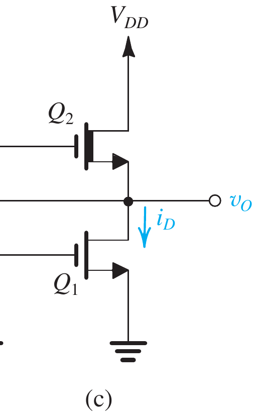
Limitation of NMOS logic: There is always a DC current path from \(V_{DD}\) to ground when the output is LOW (both load and driver are ON). This means NMOS logic has significant static power dissipation, which limits integration density.
NMOS NAND Gate
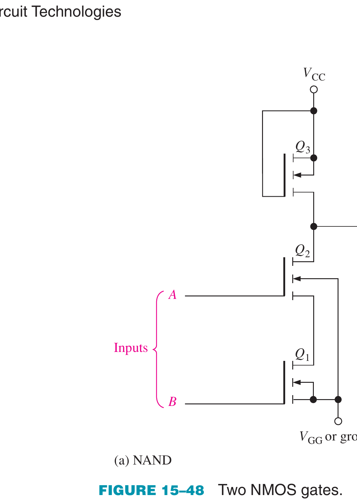
Uses series-connected enhancement NMOS transistors in the pull-down path, sharing one depletion-mode load. Output goes LOW only when all inputs are HIGH (all series transistors ON).
NMOS NOR Gate
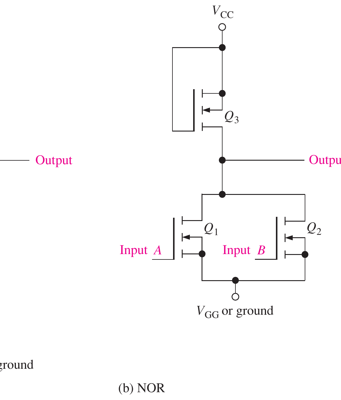
Uses parallel-connected enhancement NMOS transistors in the pull-down path, sharing one depletion-mode load. Output goes LOW when any input is HIGH (any parallel transistor ON).
CMOS Logic
CMOS Logic Definition
CMOS (Complementary Metal-Oxide-Semiconductor) logic uses complementary pairs of P-channel and N-channel MOSFETs. In every CMOS gate, there is a PMOS pull-up network (connects output to \(V_{DD}\)) and an NMOS pull-down network (connects output to ground). The two networks are complementary — when one is ON, the other is OFF. This means there is no direct DC path from \(V_{DD}\) to ground in either logic state, resulting in near-zero static power dissipation. This is the single most important advantage of CMOS.
MOSFETs as Switches — Strong and Weak Logic Levels
Inside a logic gate a MOSFET behaves as a voltage-controlled switch, with the gate-to-source voltage \(V_{GS}\) as the control:
- NMOS: ON (closed) when \(V_{GS} > V_{Tn}\); OFF (open) when \(V_{GS} < V_{Tn}\).
- PMOS: the threshold is negative — ON when \(V_{SG} > \lvert V_{Tp}\rvert\) (a LOW gate); OFF when the gate is HIGH.
The key to CMOS is that each device passes one logic level well ("strong") and the other poorly ("weak"):
- An NMOS passes a strong 0 but a weak 1. When it tries to pull a node up, the rising source voltage shrinks \(V_{GS}\); conduction stops once \(V_{GS}=V_{Tn}\), so the output cannot rise above \(V_{DD}-V_{Tn}\).
- A PMOS passes a strong 1 but a weak 0. When it tries to pull a node down, conduction stops once \(V_{SG}=\lvert V_{Tp}\rvert\), so the output cannot fall below \(\lvert V_{Tp}\rvert\).
| Device | Strong level (full) | Weak level (degraded) | Therefore used as |
|---|---|---|---|
| NMOS | Logic 0 → \(0\,\text{V}\) | Logic 1 → \(V_{DD}-V_{Tn}\) | Pull-down network |
| PMOS | Logic 1 → \(V_{DD}\) | Logic 0 → \(\lvert V_{Tp}\rvert\) | Pull-up network |
This is exactly why CMOS uses a PMOS pull-up (delivers a strong 1) and an NMOS pull-down (delivers a strong 0). The complementary pair gives rail-to-rail (full-swing) output — \(0\,\text{V}\) to \(V_{DD}\) — and hence the maximum noise margin, the decisive advantage over NMOS-only or PMOS-only logic.
CMOS Inverter — The Fundamental CMOS Gate
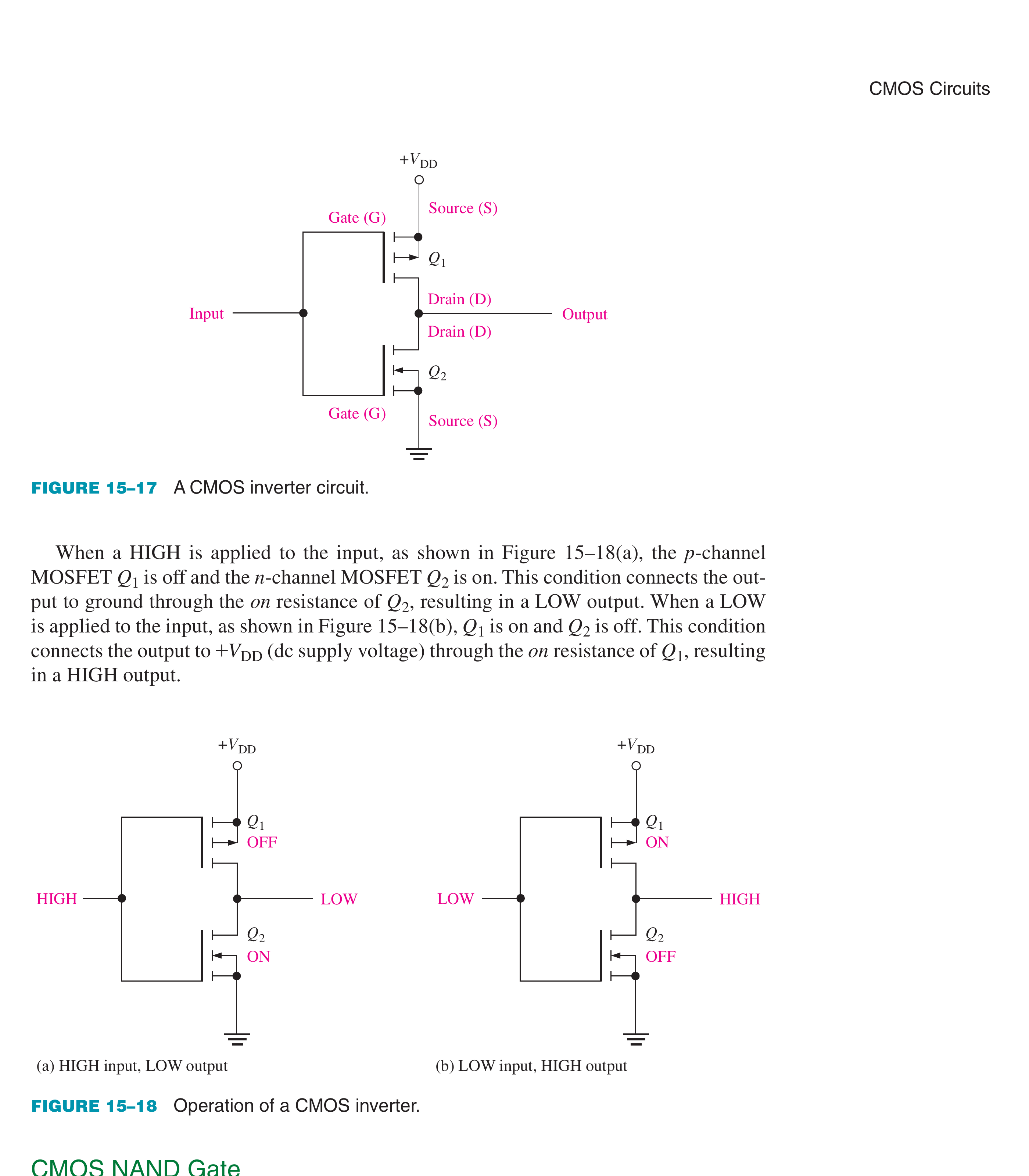
The CMOS inverter consists of one PMOS (pull-up) and one NMOS (pull-down) transistor.
Operation:
| Input (\(V_{in}\)) | NMOS | PMOS | Output (\(V_{out}\)) | Current Path |
|---|---|---|---|---|
| LOW (0 V) | OFF | ON | HIGH (\(V_{DD}\)) | No DC path (NMOS is OFF) |
| HIGH (\(V_{DD}\)) | ON | OFF | LOW (0 V) | No DC path (PMOS is OFF) |
In both stable states, one transistor is always OFF → no static current → zero static power dissipation.
Current flows only during the brief transition when both transistors are momentarily ON.
Book-grounded current-path check
In either stable logic state, one device interrupts the direct \(V_{DD}\)-to-ground path. Static CMOS power is therefore ideally leakage-only; appreciable supply current occurs mainly while both devices conduct during a transition and while capacitance is charged or discharged.
Source figure: Floyd, Digital Fundamentals (11th ed.), PDF p. 866.
CMOS Inverter — Voltage Transfer Characteristic (VTC)
The VTC shows the relationship between \(V_{in}\) and \(V_{out}\). For a symmetric CMOS inverter (matched NMOS and PMOS):
- Switching threshold: \(V_{th} = V_{DD}/2\) (midpoint transition)
- Full output swing: Output swings between \(0\,\text{V}\) and \(V_{DD}\) (rail-to-rail)
- High noise margins: \(NM_H = NM_L \approx V_{DD}/2 - V_{th(\text{transistor})}\)
The VTC has five operating regions as \(V_{in}\) sweeps from 0 to \(V_{DD}\). The sharp transition in the middle gives CMOS its excellent noise immunity.
The paired characteristics below make the technology trade-off explicit: the depletion-load NMOS switching point and LOW level depend on the driver/load ratio and a DC path remains when the driver conducts, whereas complementary CMOS gives rail-to-rail levels, a near-mid-supply switching point, and wide noise margins with negligible static current.
Transfer curve: \(V_{out}\) stays near \(V_{DD}\) for small \(V_{in}\), drops sharply at the switching threshold \(V_{in}\approx V_{DD}/2\), and settles near 0 for large \(V_{in}\) — giving rail-to-rail swing and large noise margins.
CMOS NAND Gate
Structure:
- PMOS pull-up network: Two PMOS transistors in parallel (output goes HIGH if any input is LOW → any PMOS turns ON)
- NMOS pull-down network: Two NMOS transistors in series (output goes LOW only when all inputs are HIGH → all NMOS turn ON)
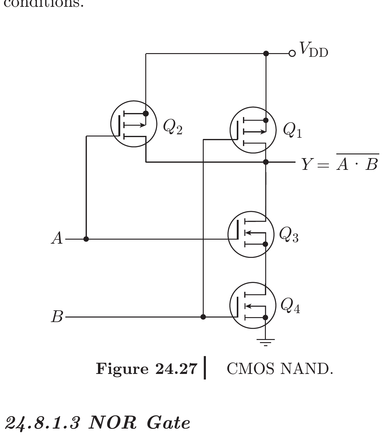
Truth Table (2-input CMOS NAND):
| \(A\) | \(B\) | PMOS Network | NMOS Network | Output |
|---|---|---|---|---|
| 0 | 0 | Both ON (parallel) | Both OFF | 1 (HIGH) |
| 0 | 1 | \(P_A\) ON | \(N_B\) ON, \(N_A\) OFF | 1 (HIGH) |
| 1 | 0 | \(P_B\) ON | \(N_A\) ON, \(N_B\) OFF | 1 (HIGH) |
| 1 | 1 | Both OFF | Both ON (series) | 0 (LOW) |
CMOS Rule for gate construction:
- NAND → NMOS in series, PMOS in parallel
- NOR → NMOS in parallel, PMOS in series
CMOS NOR Gate
Structure:
- PMOS pull-up network: Two PMOS transistors in series (output goes HIGH only when all inputs are LOW → all PMOS turn ON)
- NMOS pull-down network: Two NMOS transistors in parallel (output goes LOW if any input is HIGH → any NMOS turns ON)
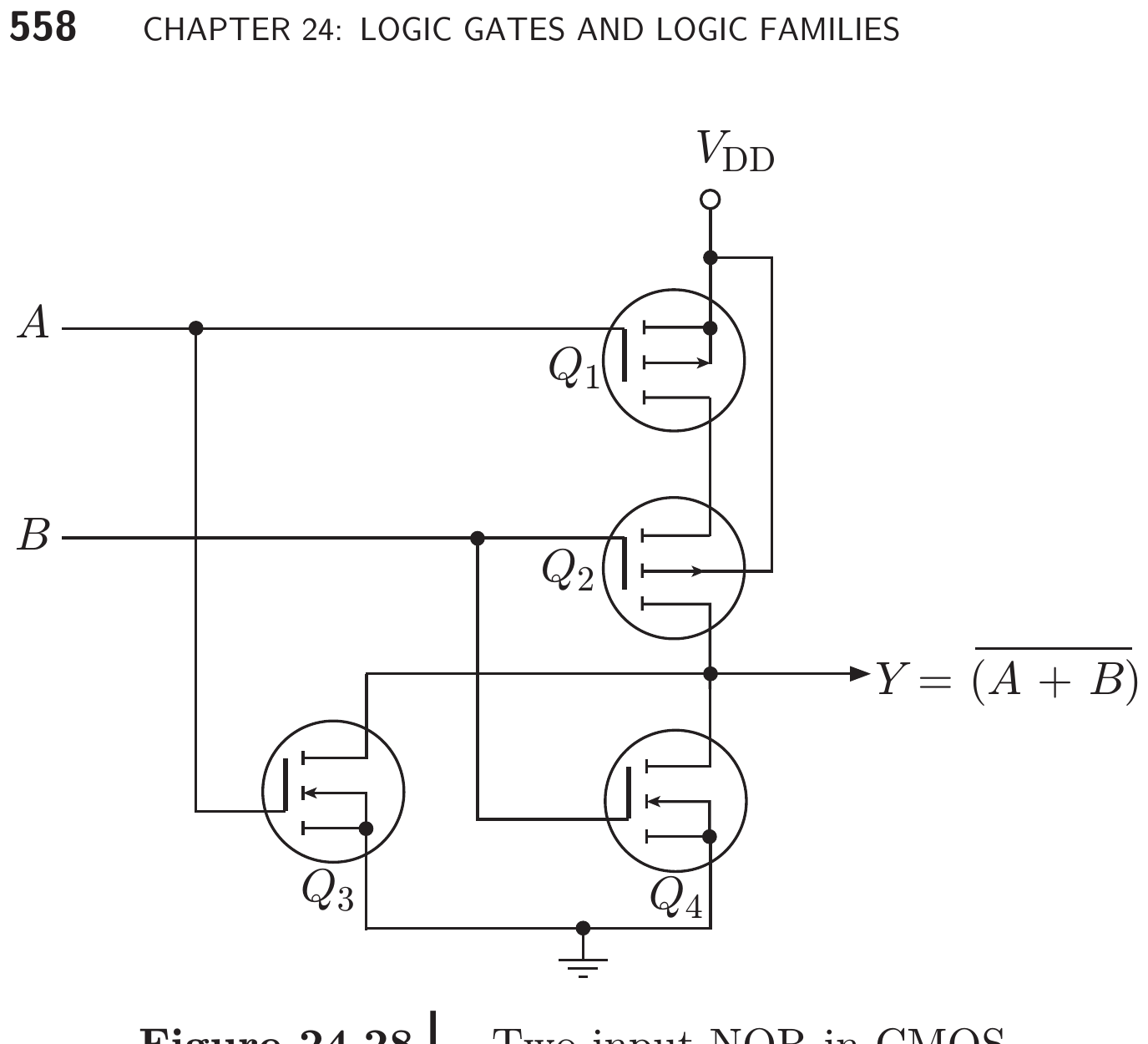
General CMOS Gate Synthesis (PUN/PDN Duality)
Every static CMOS gate computes an inverting function \(Y=\overline{f}\) using two complementary networks driven by the same inputs:
- The pull-down network (PDN, NMOS) conducts — pulling \(Y\) to \(0\) — exactly when \(f=1\). Build it directly from \(f\): an AND (\(\cdot\)) becomes NMOS in series; an OR (\(+\)) becomes NMOS in parallel.
- The pull-up network (PUN, PMOS) is the dual of the PDN: wherever the PDN is in series the PUN is in parallel, and vice-versa. It conducts — pulling \(Y\) to \(V_{DD}\) — exactly when \(f=0\).
At any instant exactly one network conducts, so there is never a DC path from \(V_{DD}\) to ground. The method extends to any fan-in and any Boolean function:
- 3-input NAND \(Y=\overline{ABC}\): 3 NMOS in series (PDN) + 3 PMOS in parallel (PUN).
- 3-input NOR \(Y=\overline{A+B+C}\): 3 NMOS in parallel (PDN) + 3 PMOS in series (PUN).
- AND-OR-Invert (AOI) functions such as \(Y=\overline{AB+C}\) map their series/parallel groups directly, realising a whole complex gate in a single stage.
Inputs are assumed available in true form; any complemented input (\(\overline{A}\)) requires an extra inverter.
CMOS AND and OR Gates
Because a CMOS gate always has an inverting pull-up/pull-down structure, its natural gates are NOT, NAND and NOR. The non-inverting AND and OR are obtained by following the inverting gate with an inverter:
- AND = CMOS NAND + inverter (6 transistors)
- OR = CMOS NOR + inverter (6 transistors)
This is why, in CMOS, NAND/NOR are cheaper than AND/OR — the opposite of what beginners expect. Designers therefore prefer NAND/NOR-based logic.
CMOS Transmission Gate (Pass Gate)
A transmission gate (TG) places an NMOS and a PMOS in parallel, driven by complementary controls \(C\) and \(\overline{C}\). When \(C = 1\) both transistors are ON and the gate passes the signal with a full \(0\)-to-\(V_{DD}\) swing (the NMOS passes a strong 0, the PMOS a strong 1); when \(C = 0\) both are OFF and the path is open (high-impedance, Hi-Z).
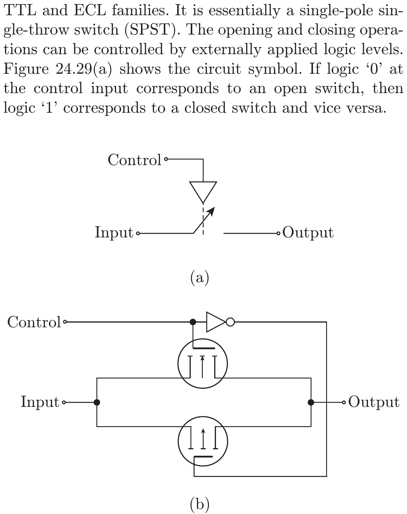
The transmission gate is the building block of CMOS multiplexers, latches and XOR/XNOR gates.
CMOS XOR / XNOR Gate
XOR and XNOR are not primitive CMOS gates — they are compound functions:
Truth table:
| \(A\) | \(B\) | XOR | XNOR |
|---|---|---|---|
| 0 | 0 | 0 | 1 |
| 0 | 1 | 1 | 0 |
| 1 | 0 | 1 | 0 |
| 1 | 1 | 0 | 1 |
Three common realisations:
- Transmission-gate XOR — a compact, high-speed CMOS style using ~6–8 transistors (2 transmission gates + inverters). Preferred inside CMOS chips.
- Universal-gate XOR — XOR built from four NAND gates (below); XNOR is then XOR followed by an inverter. Useful when only NAND gates are available.
- Direct AOI (static CMOS) — realise the complementary function as one complex gate. Since \(\text{XOR}=0\) when \(A=B\), the PDN is \((A\!\cdot\!B)\parallel(\overline{A}\!\cdot\!\overline{B})\) and the dual PUN is \((A\parallel B)\) in series with \((\overline{A}\parallel\overline{B})\) — 8 transistors plus inverters for \(\overline{A},\overline{B}\).
The direct static-CMOS (AOI) realisations use 8 transistors each (inputs plus their complements). The NMOS pull-down encodes when the output is \(0\); the PMOS pull-up is its series↔parallel dual:
XOR/XNOR are the heart of parity generators/checkers, comparators and adders (the sum bit is \(S = A \oplus B \oplus C_{in}\)).
CMOS Power Dissipation
| Component | Formula | Description |
|---|---|---|
| Static power | \(P_{static} = V_{DD} \times I_{leakage}\) | Due to sub-threshold leakage; nearly zero in older CMOS, significant in nanometer nodes |
| Dynamic power | \(P_{dynamic} = \alpha \cdot C_L \cdot V_{DD}^2 \cdot f\) | Dominant term; \(\alpha\) = activity factor, \(C_L\) = load capacitance, \(f\) = clock frequency |
| Short-circuit power | \(P_{sc} = I_{sc} \cdot V_{DD} \cdot f\) | During transitions when both NMOS and PMOS momentarily conduct |
The load capacitance \(C_L\) comes from the input (gate) capacitance of the next stage plus interconnect wiring; every output transition (\(0\!\to\!1\) or \(1\!\to\!0\)) charges or discharges it through the conducting network, dissipating \(C_L V_{DD}^2\) per cycle. The short-circuit term arises because the finite input rise/fall time leaves both transistors briefly ON.
\(P_{dynamic}\) is proportional to \(V_{DD}^2\) — this is why reducing supply voltage is the most effective way to reduce CMOS power.
Logic Family Comparison
| Parameter | TTL (74LS) | NMOS | CMOS (4000 series) | CMOS (74HC) |
|---|---|---|---|---|
| Supply voltage | \(5\,\text{V}\) only | \(5\,\text{V}\) | \(3–18\,\text{V}\) | \(2–6\,\text{V}\) |
| Static power | ~\(2\,\text{mW}\) | Significant | ~\(10\,\text{nW}\) | ~\(10\,\text{nW}\) |
| Speed (prop. delay) | ~\(10\,\text{ns}\) | ~\(10\,\text{ns}\) | ~\(50\,\text{ns}\) | ~\(8\,\text{ns}\) |
| Noise margin | \(0.4\,\text{V}\) | Moderate | \(\approx 45\%\,V_{DD}\) (excellent) | \(\approx 45\%\,V_{DD}\) |
| Fan-out | 10 | ~50 | >50 | >50 |
| Integration density | Low | High | Very high | Very high |
| Input impedance | Low | Very high | Very high | Very high |
Key Exam Points — NMOS/CMOS
- CMOS has near-zero static power because there is never a DC path from \(V_{DD}\) to ground (complementary transistors).
- NMOS passes a strong 0 / weak 1; PMOS passes a strong 1 / weak 0 — so NMOS is the pull-down and PMOS the pull-up, giving rail-to-rail swing.
- NMOS has static power dissipation because the load device is always ON.
- CMOS NAND: NMOS in series, PMOS in parallel. CMOS NOR: NMOS in parallel, PMOS in series.
- Any gate: build the PDN (NMOS) from \(f\) (AND→series, OR→parallel); the PUN (PMOS) is its dual. Complemented inputs need inverters.
- CMOS dynamic power = \(\alpha C_L V_{DD}^2 f\) → reducing \(V_{DD}\) is quadratically effective.
- CMOS has rail-to-rail output swing (0 to \(V_{DD}\)) and excellent noise margins.
- CMOS dominates modern VLSI (all modern processors, memory, SoCs are CMOS).
Model Answer — CMOS Inverter and Logic-Gate Realisation [10 marks]
Exam-ready answer
Complementary MOS (CMOS) logic uses a PMOS pull-up network (PUN) from \(V_{DD}\) to the output and a complementary NMOS pull-down network (PDN) from the output to ground. The PUN supplies a strong 1 and the PDN supplies a strong 0; in a stable state one network is OFF, so static power is ideally zero.
Inverter: the PMOS and NMOS gates share input \(A\), and their drains share output \(Y\).
| \(A\) | PMOS | NMOS | \(Y\) |
|---|---|---|---|
| 0 | ON | OFF | \(V_{DD}\) (1) |
| 1 | OFF | ON | \(0\) (0) |
Thus \(Y=\overline A\), with rail-to-rail output and no direct DC path in either stable state. Dynamic power is approximately \(P_{dyn}=\alpha C_LV_{DD}^{2}f\), where \(\alpha\) is switching activity, \(C_L\) is load capacitance (F), and \(f\) is frequency (Hz).
NAND: for \(Y=\overline{AB}\), place NMOS devices in series so both inputs must be HIGH to pull down; use the dual PUN with PMOS devices in parallel, so either LOW input pulls up.
NOR: for \(Y=\overline{A+B}\), place NMOS devices in parallel, so any HIGH pulls down; use PMOS devices in series, so only two LOW inputs pull up.
This is the general duality rule: construct the NMOS PDN from the condition \(f\) that should make the output LOW, replacing AND by series and OR by parallel; obtain the PMOS PUN by interchanging series and parallel. The resulting static gate computes \(Y=\overline f\).
Non-inverting gates: CMOS naturally gives NOT, NAND and NOR. Add one CMOS inverter after NAND to obtain AND,
and after NOR to obtain OR,
Each two-input AND or OR therefore needs six transistors: four in the NAND/NOR plus two in the inverter.
XOR:
which is 1 only for unequal inputs. It may be realised by four NAND gates, by a direct complementary AOI network, or efficiently with transmission gates. A transmission gate places NMOS and PMOS in parallel under complementary controls, combining the NMOS strong 0 with the PMOS strong 1 to pass a full-swing signal.
Example of operation: for a CMOS NAND with \(A=1,B=0\), the \(A\)-NMOS is ON but the series \(B\)-NMOS is OFF, so there is no path to ground; the \(B\)-PMOS is ON and pulls \(Y\) to \(V_{DD}\). Only \(A=B=1\) completes the PDN and gives 0.
CMOS gates provide high input impedance, wide noise margins, low static power and very high integration density. Leakage and switching power remain practical limitations, and excessive fan-in increases series resistance and propagation delay. These properties make CMOS the basis of processors, memories and system-on-chip logic.
Practice target: 16–18 minutes; draw inverter, NAND and NOR topologies and state the PUN/PDN duality before deriving AND, OR and XOR.
Model Answer — TTL, NMOS and CMOS Comparison [10 marks]
Exam-ready answer
A logic family is a compatible set of digital ICs fabricated with one circuit technology and sharing supply, logic-level, drive, delay and power specifications. TTL uses BJTs, NMOS uses only n-channel MOS devices with an always-on load, and CMOS uses complementary NMOS/PMOS networks.
| Parameter | TTL (typical 74LS) | NMOS | CMOS (4000/74HC) |
|---|---|---|---|
| Basic devices | Bipolar transistors; multi-emitter input and totem-pole output | Enhancement NMOS logic plus resistor/depletion NMOS load | Complementary PMOS PUN and NMOS PDN |
| Supply | Usually fixed \(5\,\text{V}\) | Commonly \(5\,\text{V}\) | Wide family-dependent range; 4000 about \(3\)–\(18\,\text{V}\), 74HC about \(2\)–\(6\,\text{V}\) |
| Input impedance | Relatively low; input current must be supplied/sunk | Very high, capacitive | Very high, capacitive |
| Static power | Moderate because BJTs require bias current | Significant when output is LOW because load and driver conduct | Ideally zero in stable states; practical leakage remains |
| Dynamic power | Moderate | Charges gate/load capacitance | \(P_{dyn}=\alpha C_LV_{DD}^{2}f\) |
| Propagation delay | About \(10\,\text{ns}\) for 74LS | About \(10\,\text{ns}\), process dependent | 4000 CMOS slower (about \(50\,\text{ns}\)); 74HC around \(8\,\text{ns}\) |
| Noise margin | About \(0.4\,\text{V}\) for standard 5-V TTL | Moderate and ratio dependent | Excellent, commonly a large fraction of \(V_{DD}\) |
| Fan-out | Current limited; typically 10 | Mainly capacitive, often around 50 | Very high DC fan-out; practical limit set by total gate capacitance and speed |
| Output swing | Not fully rail-to-rail; standard TTL HIGH is typically about \(3.6\,\text{V}\) | LOW and threshold depend on driver/load ratio | Nearly \(0\) to \(V_{DD}\) |
| Density | Low | High | Very high |
| ESD sensitivity | More robust | Gate oxide is sensitive | Gate oxide is sensitive; unused inputs must never float |
Circuit reason for the power difference: the NMOS load is always ON, so a LOW output creates a DC path \(V_{DD}\to\) load \(\to\) driver \(\to\) ground. In CMOS, a LOW input turns PMOS ON/NMOS OFF and a HIGH input does the reverse, eliminating the ideal steady DC path. TTL continuously biases bipolar stages and therefore also consumes static power.
Figures of merit: propagation delay \(t_{pd}\) measures switching speed. The speed-power product is
and lower is better. For example, a 74LS gate with \(P_D=2\,\text{mW}\) and \(t_{pd}=9.5\,\text{ns}\) has \(SPP=19\,\text{pJ}\). Fan-out is current-limited in TTL:
whereas in MOS logic the very small DC gate current gives high fan-out but each added input capacitance slows transitions.
Selection and applications: TTL gives strong output drive, robust interfacing and predictable 5-V levels, so it remains useful in legacy 7400 control hardware. NMOS offered better density than TTL and powered early microprocessors but wastes static power and is ratioed. CMOS combines high density, rail-to-rail swing, high noise immunity and very low static power; voltage scaling also reduces dynamic power quadratically. Modern high-speed CMOS has removed its historical speed disadvantage, so it dominates VLSI processors, memories and portable systems.
No family is chosen from speed alone: supply compatibility, capacitive loading, noise environment, power budget and interface current must all be checked.
Practice target: 16–18 minutes; reproduce the comparison table, derive SPP and fan-out, and finish with technology selection.