Semiconductor Memory
Possible Exam Questions
Exam Questions and Answer Map
Questions marked [PYQ paper/year] were directly observed in past papers; [likely] means pattern-based prediction, not a claimed past question. Rehearse each answer plan closed-book, then check the full answer via the links.
-
Classify semiconductor memories; differentiate RAM and ROM. [5] — [likely]
-
Answer plan: Draw the volatile/non-volatile tree → place SRAM/DRAM under RAM and PROM/EPROM/EEPROM/Flash under ROM → compare access and retention.
-
Model answer: Semiconductor-Memory Classification and RAM–ROM Comparison
-
Differentiate SRAM and DRAM; why does DRAM need refreshing? [5] — [likely]
-
Answer plan: Compare 6T latch with 1T1C cell → speed, density, cost and read type → explain capacitor leakage and periodic refresh.
-
Model answer: SRAM, DRAM and the Need for Refresh
-
Differentiate PROM, EPROM, EEPROM and Flash memory. [5] — [likely]
-
Answer plan: Compare programming method, erasure method and granularity → distinguish NOR and NAND Flash applications.
- Model answer: PROM, EPROM, EEPROM and Flash Memory
1. Semiconductor Memory
Likely Exam Question (10 marks)
"Classify semiconductor memories. Compare SRAM and DRAM with respect to speed, density, cost, and applications." OR "Explain different types of ROM: PROM, EPROM, EEPROM, and Flash memory."
Definition
Semiconductor memory is an electronic data storage device fabricated on silicon integrated circuits. It stores binary data (0s and 1s) in large arrays of memory cells.
Classification of Semiconductor Memory
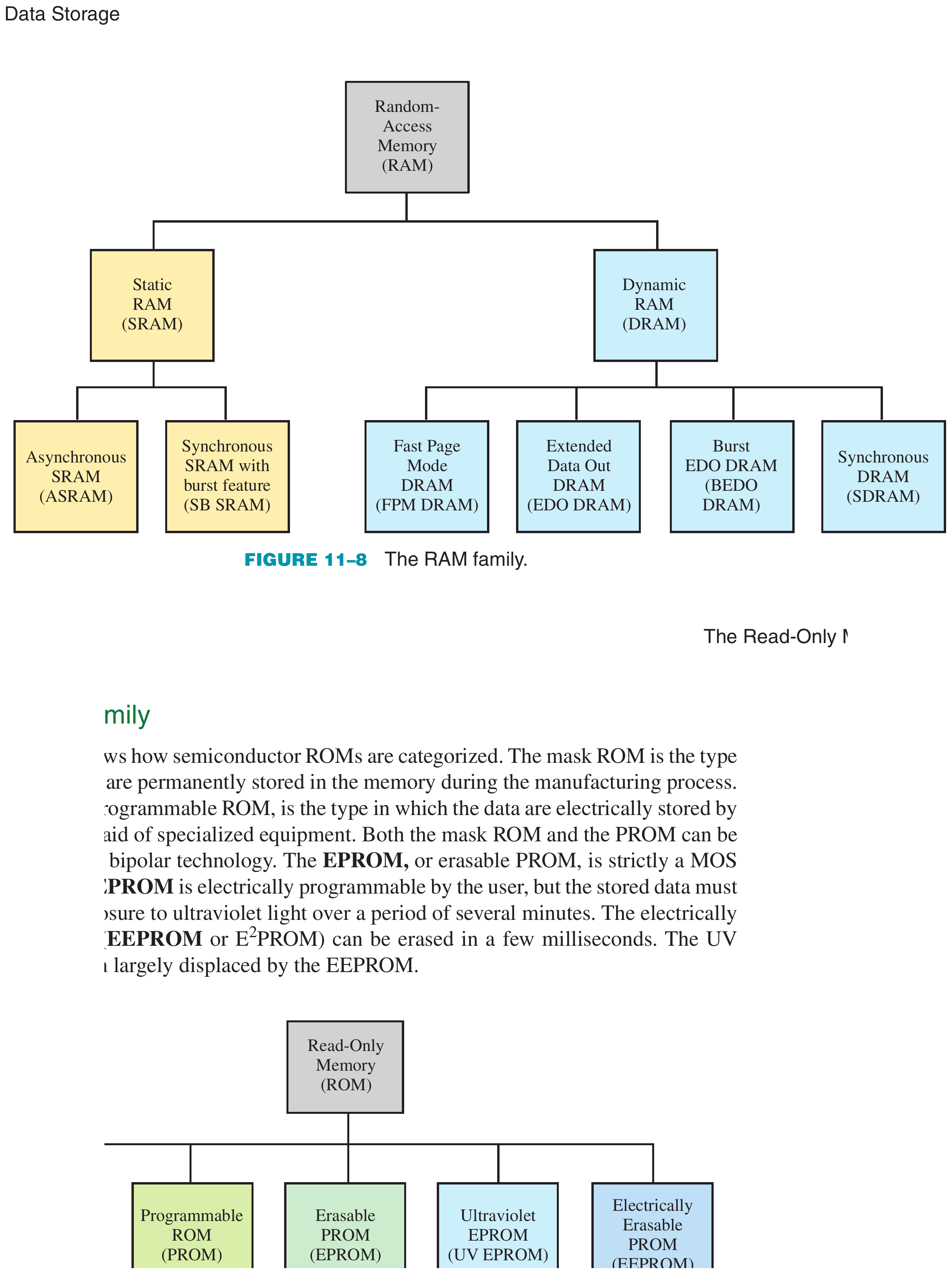
Volatile memory loses data when power is removed. Non-volatile memory retains data without power.
Array Organization
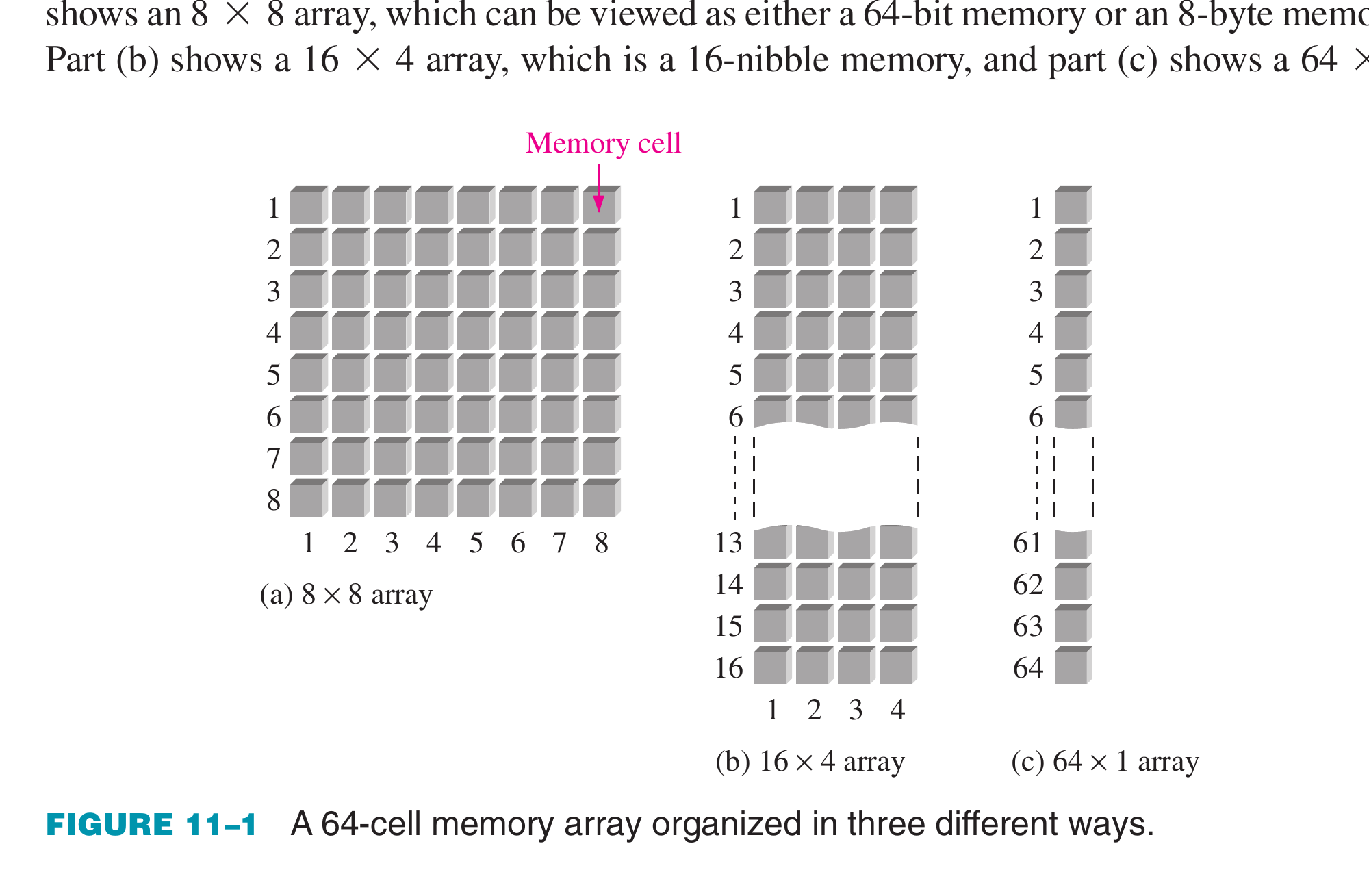
Book-grounded capacity rule
Memory capacity is number of words × bits per word. The three shown organizations all store 64 bits: \(8\times8\), \(16\times4\), and \(64\times1\). Organization changes the address width and data-word width, not total stored bits.
Source figure: Floyd, Digital Fundamentals (11th ed.), PDF p. 629.
RAM — Random Access Memory
Definition: RAM is a volatile read/write memory where any location can be accessed in the same amount of time regardless of its physical location (hence "random access"). Data is lost when power is switched off.
Static RAM (SRAM)
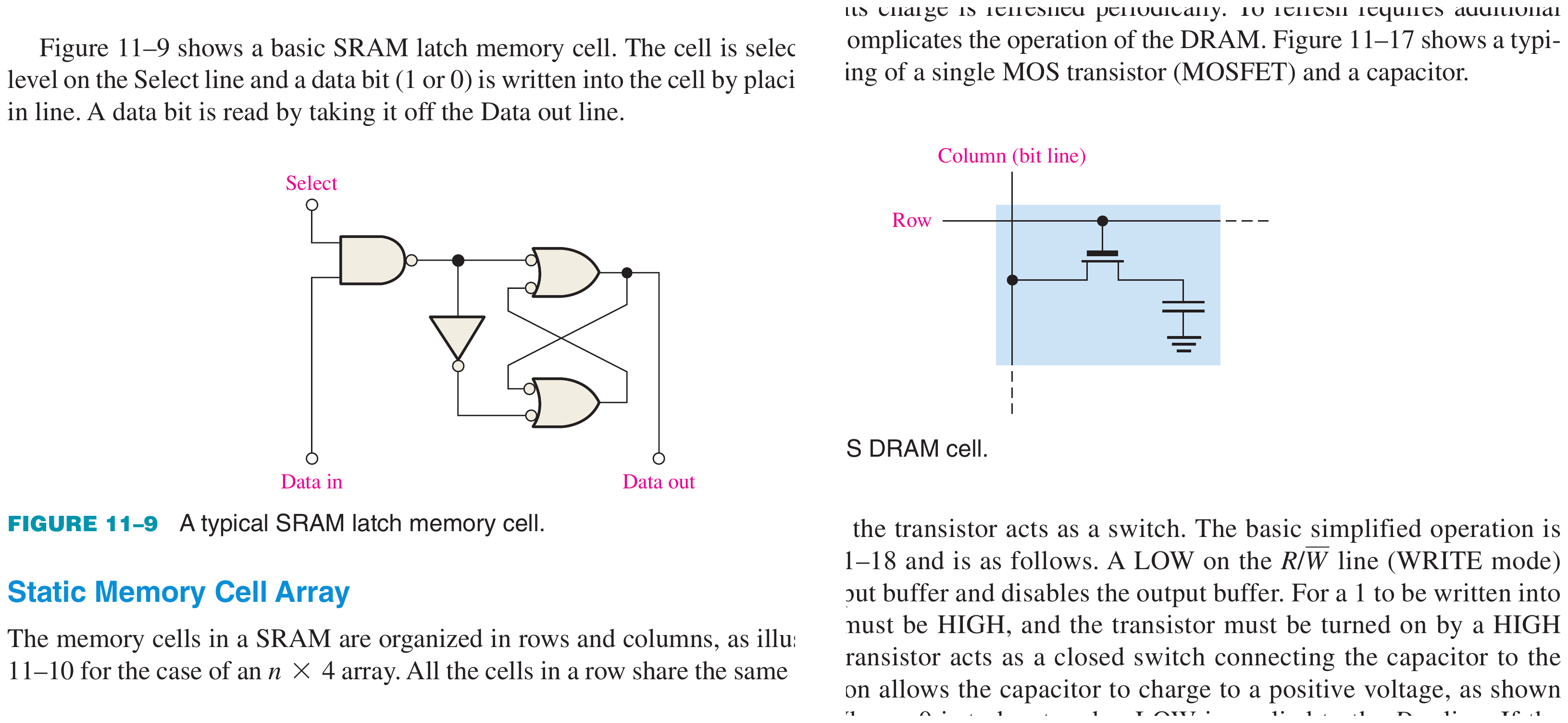
Definition: SRAM uses a cross-coupled latch (typically 6 transistors per cell: two cross-coupled inverters + two access transistors) to store each bit. Data is retained as long as power is supplied — no refresh needed.
SRAM cell structure (6T):
- Two cross-coupled CMOS inverters form a bistable latch (stores 0 or 1).
- Two NMOS access transistors controlled by the word line.
- Read: word line activates → bit lines sense the stored value.
- Write: word line activates → external drivers force new value onto bit lines.
Key characteristics:
- Fast (access time: 1–10 ns for modern SRAM)
- Low density (6 transistors per bit → large cell area)
- High cost per bit
- No refresh needed
- Low power (static current only)
Applications: CPU cache (L1, L2, L3), register files, high-speed buffers.
Dynamic RAM (DRAM)
Definition: DRAM stores each bit as a charge on a tiny capacitor (1 transistor + 1 capacitor per cell). The capacitor charge leaks over time, so DRAM requires periodic refresh (re-reading and re-writing every row, typically every 64 ms).
DRAM cell structure (1T1C):
- One NMOS access transistor + one storage capacitor.
- Logic 1: capacitor charged. Logic 0: capacitor discharged.
- Read is destructive — the charge on the capacitor is disturbed during reading. Data must be written back (refresh) after every read.
Key characteristics:
- Slower than SRAM (access time: 50–70 ns for modern DRAM)
- High density (1 transistor per bit → very compact)
- Low cost per bit
- Refresh required (every 64 ms typically)
- Higher power (due to refresh circuitry)
Applications: Main memory (RAM) of computers, smartphones, embedded systems.
SRAM vs DRAM — Comparison
| Feature | SRAM | DRAM |
|---|---|---|
| Cell structure | 6 transistors (latch) | 1 transistor + 1 capacitor |
| Speed | Very fast (1–10 ns) | Slower (50–70 ns) |
| Density | Low (large cell) | High (small cell) |
| Cost per bit | High | Low |
| Refresh | Not needed | Required (every ~64 ms) |
| Power consumption | Low (static) | Higher (refresh overhead) |
| Read operation | Non-destructive | Destructive (needs refresh) |
| Application | Cache memory | Main memory |
ROM — Read-Only Memory
Definition: ROM is a non-volatile memory in which data is permanently or semi-permanently stored. Data can be read at any time but is written (programmed) only once or through a special process.
Mask ROM
Factory-programmed during IC fabrication. Data is built into the silicon mask pattern. Cannot be modified. Lowest cost in high volume. Used for fixed programs (firmware in appliances, game cartridges).
PROM (Programmable ROM)
Definition: PROM is a one-time programmable ROM. It is manufactured with all bits set to 1 (or 0). The user programs it by selectively blowing fusible links (fuses) using a PROM programmer. Once a fuse is blown, the bit is permanently changed. Cannot be erased or reprogrammed.
EPROM (Erasable Programmable ROM)
Definition: EPROM uses floating-gate MOSFET transistors. Data is programmed by injecting charge onto the floating gate using hot electron injection (high voltage, ~12.5V). The trapped charge shifts the threshold voltage, changing the stored bit.
Erasure: Exposure to ultraviolet (UV) light through a quartz window on the IC package erases the entire chip (takes 15–20 minutes). Erasure is not selective — the entire chip is erased.
Common IC: 2716 (2K × 8), 2732 (4K × 8), 27256 (32K × 8).
EEPROM (Electrically Erasable Programmable ROM)
Definition: EEPROM can be electrically erased and reprogrammed at the byte level without removing the chip from the circuit. Uses Fowler-Nordheim tunnelling to add or remove charge from the floating gate.
Key advantages over EPROM:
- Erasable electrically (no UV needed).
- Selective erasure (byte-by-byte).
- In-circuit programming.
Disadvantage: Slower write speed, limited write endurance (~100,000 to 1 million write cycles per byte).
Flash Memory
Definition: Flash memory is a type of EEPROM that can be erased and reprogrammed in large blocks (sectors) rather than byte-by-byte. This makes it much faster for bulk writes than standard EEPROM.
Two architectures:
- NOR Flash: Random access (like RAM), fast reads, suitable for code execution (XIP — execute in place). Used in firmware, BIOS.
- NAND Flash: Sequential access, higher density, faster writes/erases. Used in USB drives, SSDs, memory cards, smartphones.
Applications: USB flash drives, solid-state drives (SSDs), SD cards, smartphone storage, firmware.
ROM Types — Comparison
| Type | Programmable By | Erasable | Erasure Method | Granularity |
|---|---|---|---|---|
| Mask ROM | Factory | No | — | — |
| PROM | User (once) | No | — | — |
| EPROM | User | Yes | UV light | Entire chip |
| EEPROM | User | Yes | Electrical | Byte-level |
| Flash | User | Yes | Electrical | Block/sector-level |
Key Exam Points — Memory
- SRAM: fast, expensive, 6T cell, no refresh → cache. DRAM: dense, cheap, 1T1C cell, needs refresh → main memory.
- DRAM read is destructive; SRAM read is non-destructive.
- EPROM: UV erasure (entire chip). EEPROM: electrical erasure (byte level). Flash: electrical (block level).
- Flash memory has two types: NOR (fast read, code execution) and NAND (high density, storage).
Model Answer — Semiconductor-Memory Classification and RAM–ROM Comparison [5 marks]
Exam-ready answer
Semiconductor memory is an integrated-circuit array that stores binary information in electronic cells addressed by row and column circuitry. It is classified primarily by whether data survives removal of power and by whether normal operation permits writing.
- Volatile read/write memory (RAM): SRAM, which stores a bit in a bistable latch, and DRAM, which stores charge on a capacitor.
- Non-volatile memory (ROM family): mask ROM, one-time-programmable PROM, UV-erasable EPROM, electrically byte-erasable EEPROM, and electrically block-erasable Flash.
| Point | RAM | ROM / non-volatile family |
|---|---|---|
| Full meaning | Random Access Memory | Read-Only Memory |
| Retention | Volatile; loses data without supply | Retains data without supply |
| Normal operation | Frequent read and write; approximately uniform access time for any address | Mainly read; programming/erasure is absent or slower and uses a special procedure |
| Cell examples | 6T latch in SRAM; 1T1C charge cell in DRAM | Mask connection, fuse, or floating-gate transistor |
| Speed and endurance | Fast writes and effectively unlimited normal read/write cycles | Reads are fast, but erase/write latency and finite endurance apply to EEPROM/Flash |
| Main applications | Working storage: CPU cache, registers and main memory | Firmware, boot code, calibration data and mass non-volatile storage |
“Random access” describes address access and does not itself mean volatility; many ROMs are also randomly readable. Likewise, Flash is placed in the ROM/non-volatile family even though it is rewritable, because it retains programmed threshold states without power and is erased in blocks rather than written like RAM.
Conclusion: RAM provides fast temporary workspace, whereas the ROM family provides persistent storage. A computer therefore combines SRAM cache, DRAM main memory and non-volatile Flash/ROM according to speed, cost and retention needs.
Practice target: 8–9 minutes; draw the classification tree and reproduce the six-point RAM–ROM table.
Model Answer — SRAM, DRAM and the Need for Refresh [5 marks]
Exam-ready answer
SRAM stores each bit as one of two stable states of a cross-coupled latch, whereas DRAM stores each bit as charge on a small capacitor. Both are volatile, but only DRAM needs periodic refresh.
| Feature | SRAM | DRAM |
|---|---|---|
| Cell | Usually 6 MOSFETs: two cross-coupled inverters plus two access transistors | One access transistor and one storage capacitor (1T1C) |
| Stored state | Regenerative latch voltage | Capacitor charged for 1, discharged for 0 |
| Read | Non-destructive; latch reinforces its state | Destructive/charge-sharing read; sense amplifier must restore the bit |
| Refresh | Not required while power is present | Every row must be sensed and rewritten within its retention time |
| Speed | Very fast, typically nanoseconds | Slower because bit-line sensing, precharge and restore are required |
| Area/cost | Large cell, lower density, high cost per bit | Tiny cell, high density, low cost per bit |
| Use | CPU caches and register files | Large-capacity main memory |
Why DRAM refresh is necessary: the capacitor is not ideal. Junction leakage, subthreshold leakage and dielectric leakage gradually remove its charge, so the voltage difference representing 1 shrinks until the sense amplifier can no longer distinguish it from 0. In addition, reading shares the small cell charge with a much larger bit-line capacitance and disturbs the stored value. A memory controller therefore activates each row and the sense amplifiers rewrite the detected values, commonly completing all rows within about \(64\,\text{ms}\).
If a DRAM has \(N_r\) rows and retention interval \(T_r\) seconds, the controller must issue refreshes at an average rate
For \(N_r=8192\) and \(T_r=64\,\text{ms}\), \(f_{ref}=128{,}000\) rows/s, or one row every \(7.8125\,\mu\text{s}\). Refresh occupies time and consumes power, but enables DRAM's much greater density.
Practice target: 8–9 minutes; draw both cells, give the comparison, and explain leakage plus destructive read.
Model Answer — PROM, EPROM, EEPROM and Flash Memory [5 marks]
Exam-ready answer
PROM, EPROM, EEPROM and Flash are non-volatile semiconductor memories: they retain bits without power but differ in how the storage element is programmed, erased and rewritten.
| Type | Storage/programming method | Erasure and granularity | In-circuit rewriting | Typical use |
|---|---|---|---|---|
| PROM | Programmer irreversibly blows selected fuse/antifuse links | Not erasable; one-time programmable | No | Permanent low-volume configuration |
| EPROM | High-voltage hot-electron injection charges floating-gate MOSFETs | UV light through package window; entire chip, typically 15–20 min | Normally removed from circuit | Development-era firmware |
| EEPROM | Electrical tunnelling adds/removes floating-gate charge | Electrical, usually byte-level | Yes | Calibration, settings and small configuration data |
| Flash | Floating-gate or charge-trap cells programmed electrically | Electrical, but erase is by sector/block | Yes | Firmware, memory cards, USB drives and SSDs |
In floating-gate devices, trapped charge changes transistor threshold voltage; approximately
where \(Q_{FG}\) is stored charge (C) and \(C_{eff}\) is effective floating-gate capacitance (F). A read circuit interprets the resulting conducting or non-conducting state as a bit. Programming/erasing stresses the dielectric, so EEPROM and Flash have finite endurance, unlike ordinary RAM writes.
Flash architectures: NOR Flash has random, fast reads and supports execute-in-place, so it stores boot/firmware code. NAND Flash connects cells in strings, giving higher density and faster block programming/erasure but requiring page access, error correction and bad-block management; it is preferred for SSD and removable storage.
Thus the progression is: PROM cannot erase; EPROM erases the whole chip optically; EEPROM erases electrically by byte; Flash trades byte erasure for denser, faster block operation.
Practice target: 8–9 minutes; write the four-row comparison and end with NOR-versus-NAND Flash.