TTL Logic Circuits
Possible Exam Questions
Exam Questions and Answer Map
Questions marked [PYQ paper/year] were directly observed in past papers; [likely] means pattern-based prediction, not a claimed past question. Rehearse each answer plan closed-book, then check the full answer via the links.
-
Describe the operation of a TTL NAND gate; extend the idea to a TTL NOR gate and inverter. [10] — [likely]
-
Answer plan: Draw the multi-emitter input, phase splitter and totem-pole output → explain all-HIGH and any-LOW cases → contrast NOR and inverter structures.
-
Model answer: TTL NAND, NOR and Inverter Operation
-
Explain TTL totem-pole, open-collector and tri-state outputs. [10] — [likely]
-
Answer plan: State the switching devices in each output → explain active pull-up/pull-down → show wire-AND for open collector → explain Hi-Z bus sharing.
- Model answer: TTL Output Configurations
TTL (Transistor-Transistor Logic) Circuits
Likely Exam Question (10 marks)
"Draw and explain the operation of a standard TTL NAND gate. Discuss its voltage levels, noise margins, and output configurations." OR "Compare different TTL sub-families with their speed-power products."
Definition
TTL (Transistor-Transistor Logic) is a family of digital integrated circuits built using bipolar junction transistors (BJTs). It is called "transistor-transistor" because transistors perform both the logic function (input stage) and the output drive function. The standard TTL family is the 7400 series, operating at a supply voltage of \(V_{CC} = 5\,\text{V} \pm 5\%\). TTL uses a unique multi-emitter transistor at the input stage to perform the AND logic function directly.
Standard TTL NAND Gate — Circuit Structure
The standard TTL NAND gate consists of four functional stages:
| Stage | Component | Function |
|---|---|---|
| 1. Input stage | Multi-emitter transistor \(Q_1\) | Performs AND logic using multiple emitter junctions |
| 2. Phase splitter | Transistor \(Q_2\) | Converts single signal into complementary (inverted and non-inverted) drive signals |
| 3. Pull-up (source) | Transistor \(Q_3\) + Diode \(D\) | Sources current to load, pulls output HIGH |
| 4. Pull-down (sink) | Transistor \(Q_4\) | Sinks current from load, pulls output LOW |
Stages 3 and 4 together form the totem-pole output.
The multi-emitter input transistor. Picture \(Q_1\) as several transistors with their bases tied together and collectors tied together, but each keeping a separate emitter — one per input. In silicon this is fabricated as a single transistor with two (or more) emitter regions sharing one base–collector junction. Each emitter is an independent base–emitter diode: if any input is LOW, that emitter conducts and steers \(Q_1\)'s base current out to that input. The number of emitters therefore equals the number of NAND inputs.
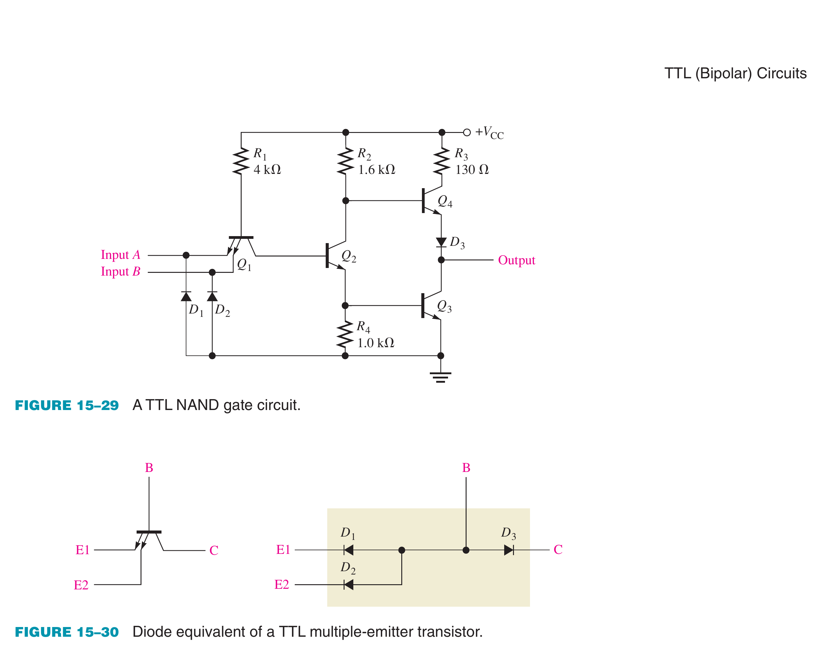
Book-grounded circuit-reading shortcut
Replace each emitter-base junction of \(Q_1\) mentally by an input diode. Any LOW input forward-biases one path and removes drive from \(Q_2\); only when all inputs are HIGH does current reach the phase splitter and pull-down chain. This gives NAND action before detailed voltage calculations.
Source figure: Floyd, Digital Fundamentals (11th ed.), PDF p. 872.
Operation — All Inputs HIGH (\(A = B = 1\))
- Both emitters of \(Q_1\) are reverse-biased (inputs are at HIGH voltage). The base of \(Q_1\) is clamped at \(\approx 2.1\,\text{V}\), so \(Q_1\) works in the reverse-active region.
- Current flows from \(V_{CC}\) through \(R_1\) and through the B-C junction of \(Q_1\) (acting as a forward-biased diode) into the base of \(Q_2\).
- \(Q_2\) turns ON → its collector drops LOW (turns OFF \(Q_3\)), its emitter rises (turns ON \(Q_4\)).
- \(Q_2\) and \(Q_4\) saturate → Output = LOW (\(V_{OL} = V_{CE(sat)} \approx 0.2\,\text{V}\)); \(Q_3\) is OFF.
Logic result: \(A=B=1 \Rightarrow Y=0\) after NAND inversion.
Operation — Any Input LOW (\(A = 0\) or \(B = 0\))
- The LOW input (\(\approx 0.2\,\text{V}\)) forward-biases its emitter of \(Q_1\), so the base of \(Q_1\) sits at only \(\approx 0.9\,\text{V}\) — too low to forward-bias a HIGH emitter (held at \(\approx 3.6\,\text{V}\)). Current is steered out of the LOW input and \(Q_1\)'s collector falls to \(\approx 0.3\,\text{V}\).
- This starves the base of \(Q_2\), so \(Q_2\) — and hence \(Q_4\) — stays OFF.
- With \(Q_2\) and \(Q_4\) off, the base of \(Q_3\) rises to \(\approx V_{CC}\) → \(Q_3\) turns ON.
- \(Q_3\) conducts → Output = HIGH (\(V_{OH} \approx V_{CC} - V_{BE3} - V_D = 5 - 1.4 \approx 3.6\,\text{V}\)).
Logic result: at least one LOW input \(\Rightarrow Y=1\).
Operation summary (2-input NAND):
| \(A\) | \(B\) | \(Q_1\) | \(Q_2\) | \(Q_3\) | \(Q_4\) | \(V_{out}\) |
|---|---|---|---|---|---|---|
| 0 | 0 | both emitters fwd (sat) | OFF | ON | OFF | HIGH ≈ 3.6 V |
| 0 | 1 | A-emitter fwd (sat) | OFF | ON | OFF | HIGH ≈ 3.6 V |
| 1 | 0 | B-emitter fwd (sat) | OFF | ON | OFF | HIGH ≈ 3.6 V |
| 1 | 1 | reverse-active | sat | OFF | sat | LOW ≈ 0.2 V |
TTL Inverter (NOT Gate)
A TTL inverter is a NAND gate with a single-emitter input transistor \(Q_1\) (instead of the multi-emitter used for NAND). The rest of the circuit — phase splitter \(Q_2\) and totem-pole output (\(Q_3\), level-shift diode \(D\), \(Q_4\)) — is identical to the NAND.
- Input HIGH → the \(Q_1\) base–collector junction feeds \(Q_2\) → \(Q_2\) and \(Q_4\) turn ON → output LOW.
- Input LOW → the \(Q_1\) emitter conducts and starves \(Q_2\) → \(Q_3\) turns ON → output HIGH.
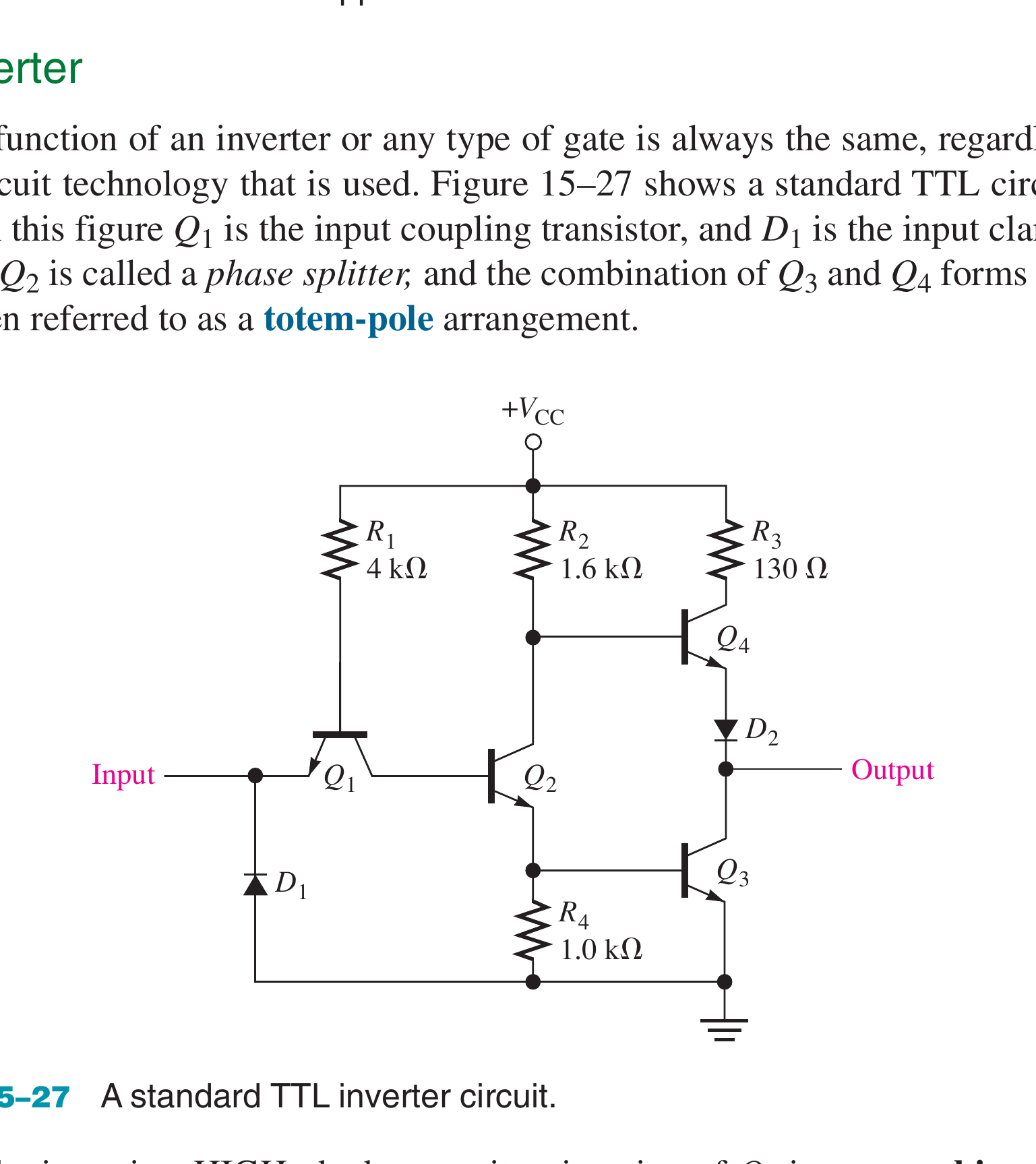
TTL Inverter — Voltage Transfer Characteristic (VTC)
The inverter is best understood through its three functional blocks and how each behaves as the input is swept from 0 to 5 V.
- Current-steering input (\(Q_1\)). \(Q_1\) steers the current one of two ways. Input LOW → the base–emitter junction conducts and current flows out of the input (away from \(Q_2\)'s base), so \(Q_2\) stays off. Input HIGH → the emitter junction reverse-biases, \(Q_1\) enters the reverse-active region, and the same current is redirected into \(Q_2\)'s base through the forward-biased base–collector junction.
- Phase splitter (\(Q_2\)). Generates two complementary drives: as its collector voltage (→ \(Q_3\)) falls, its emitter voltage (→ \(Q_4\)) rises, and vice-versa. This guarantees the two output transistors are driven in opposition.
- Totem-pole output (\(Q_3\) + level-shift diode \(D\), stacked over \(Q_4\)). A push–pull pair: \(Q_3\) sources current to pull the output HIGH, \(Q_4\) sinks current to pull it LOW. Only one is ever on, so the output is actively driven in both states.
Sweeping \(V_{in}\) from 0 to 5 V produces four regions, each fixed by the state of the four transistors:
| Region | \(V_{in}\) | \(Q_1\) | \(Q_2\) | \(Q_3\) | \(Q_4\) | Output \(V_{out}\) |
|---|---|---|---|---|---|---|
| I | \(0\)–\(0.6\,\text{V}\) | saturation | OFF | ON (active) | OFF | HIGH ≈ 3.6 V |
| II | \(0.6\)–\(1.2\,\text{V}\) | saturation | ON (active) | ON (active) | OFF | falls gently, 3.6 → ~2.2 V |
| III | \(1.2\)–\(1.5\,\text{V}\) | saturation | active → sat | ON → OFF | turns ON | falls sharply → ~0.2 V |
| IV | \(> 1.5\,\text{V}\) | reverse-active | saturation | OFF | saturation | LOW ≈ 0.2 V |
Why the breakpoints fall where they do:
- \(V_{in} < 0.6\,\text{V}\): \(Q_2\)'s base sits below \(0.7\,\text{V}\), so \(Q_2\) (and hence \(Q_4\)) stays off. \(Q_3\) conducts in the active region and holds the output at \(V_{OH} \approx V_{CC} - V_{BE3} - V_D \approx 3.6\,\text{V}\).
- \(V_{in} \approx 0.6\,\text{V}\): \(Q_2\) turns on and starts drawing collector current, so the drop across \(R_2\) rises and the output begins to fall. \(Q_4\) is still off (its emitter-resistor drop is \(< 0.7\,\text{V}\)), so the fall is gentle.
- \(V_{in} \approx 1.2\,\text{V}\): the emitter-resistor drop reaches \(\approx 0.65\,\text{V}\) and \(Q_4\) turns on. It now loads \(Q_2\)'s emitter too, so \(Q_2\)'s current climbs fast, the \(R_2\) drop grows, \(Q_3\) turns off, and the output falls sharply.
- \(V_{in} \approx 1.5\,\text{V}\): \(Q_2\) and \(Q_4\) both saturate and the output settles at \(V_{OL} \approx 0.2\,\text{V}\). The base of \(Q_1\) is now clamped at \(\approx 2.1\,\text{V}\), so any further rise in \(V_{in}\) reverse-biases \(Q_1\)'s base–emitter junction — \(Q_1\) enters the reverse-active region.
Only one output transistor conducts
Because the phase splitter drives them in antiphase, \(Q_3\) (pull-up) and \(Q_4\) (pull-down) are never both fully on. In the HIGH state \(Q_3\) sources current; in the LOW state \(Q_4\) sinks it. This active push–pull output is what gives TTL its speed and drive strength.
TTL NOR Gate
A TTL NOR gate uses two parallel input/phase-splitter branches (\(Q_{1A}\)–\(Q_{2A}\) and \(Q_{1B}\)–\(Q_{2B}\)) that share one totem-pole output. Each input has its own single-emitter current-steering transistor; the two phase-splitters are wired in parallel — collectors tied together (→ base of pull-up \(Q_3\)) and emitters tied together (→ base of pull-down \(Q_4\)). So if either input is HIGH, its phase splitter turns on, sinks current through the totem-pole and drives the output LOW.
Truth table:
| \(A\) | \(B\) | \(Y = \overline{A+B}\) |
|---|---|---|
| 0 | 0 | 1 |
| 0 | 1 | 0 |
| 1 | 0 | 0 |
| 1 | 1 | 0 |
How it works. Each input has its own current-steering transistor (\(Q_{1A}\), \(Q_{1B}\)); their phase-splitters (\(Q_{2A}\), \(Q_{2B}\)) are wired in parallel — collectors tied together (→ base of pull-up \(Q_3\)) and emitters tied together (→ base of pull-down \(Q_4\)). So either splitter, acting alone, can pull the output LOW:
- Both inputs 0 — \(Q_{1A}\), \(Q_{1B}\) steer their current out to the inputs, so \(Q_{2A}\), \(Q_{2B}\) are OFF. Their common collector rises to \(\approx V_{CC}\) → \(Q_3\) ON, \(Q_4\) OFF → output HIGH ≈ 3.6 V.
- Both inputs 1 — \(Q_{1A}\), \(Q_{1B}\) go reverse-active, driving \(Q_{2A}\), \(Q_{2B}\) into saturation → \(Q_4\) saturates → output LOW ≈ 0.2 V; \(Q_3\) OFF.
- One input HIGH (e.g. \(A=0\), \(B=1\)) — \(Q_{1A}\) forward-biased → \(Q_{2A}\) OFF, but \(Q_{1B}\) reverse-active → \(Q_{2B}\) saturates → \(Q_4\) ON → output LOW ≈ 0.2 V. A single HIGH input is enough to force the output LOW.
Operation summary (2-input NOR):
| \(A\) | \(B\) | \(Q_{2A}\) | \(Q_{2B}\) | \(Q_3\) | \(Q_4\) | \(V_{out}\) |
|---|---|---|---|---|---|---|
| 0 | 0 | OFF | OFF | ON | OFF | HIGH ≈ 3.6 V |
| 0 | 1 | OFF | sat | OFF | sat | LOW ≈ 0.2 V |
| 1 | 0 | sat | OFF | OFF | sat | LOW ≈ 0.2 V |
| 1 | 1 | sat | sat | OFF | sat | LOW ≈ 0.2 V |
Contrast with NAND: TTL NAND puts the AND function inside a single multi-emitter input transistor, whereas TTL NOR needs duplicated branches in parallel — so a TTL NOR costs more transistors than a NAND. (This is the opposite of CMOS, where NAND and NOR cost the same.)
AND and OR in TTL
TTL naturally produces the inverting gates (NAND, NOR, NOT). The non-inverting gates are made by adding an inverter stage:
- AND = NAND + inverter → \(Y = \overline{\overline{A\cdot B}} = A\cdot B\)
- OR = NOR + inverter → \(Y = \overline{\overline{A+B}} = A + B\)
More complex functions are efficiently realised as a single AND-OR-INVERT (AOI) gate (e.g. the 7451), which merges the AND, OR and inverting stages into one circuit for lower delay and fewer transistors.
TTL Voltage Levels and Noise Margins
| Parameter | Symbol | Value | Meaning |
|---|---|---|---|
| Supply voltage | \(V_{CC}\) | \(5\,\text{V} \pm 5\%\) | DC power supply |
| Minimum input HIGH | \(V_{IH}\) | \(\geq 2.0\,\text{V}\) | Any voltage above this is guaranteed to be read as HIGH |
| Maximum input LOW | \(V_{IL}\) | \(\leq 0.8\,\text{V}\) | Any voltage below this is guaranteed to be read as LOW |
| Minimum output HIGH | \(V_{OH}\) | \(\geq 2.4\,\text{V}\) | Gate produces at least this voltage for HIGH output |
| Maximum output LOW | \(V_{OL}\) | \(\leq 0.4\,\text{V}\) | Gate produces at most this voltage for LOW output |
Noise Margins — the amount of noise voltage that can be tolerated without changing the logic state:
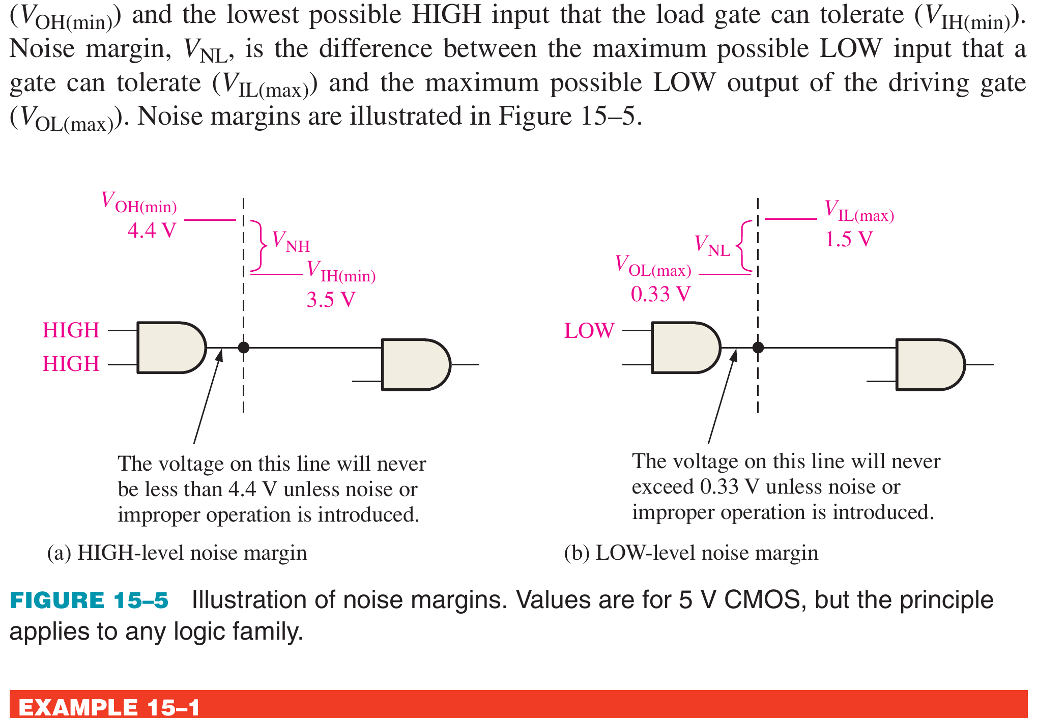
Propagation delay: Approximately \(10\,\text{ns}\) for standard TTL.
Power per gate: Approximately \(10\,\text{mW}\) for standard TTL.
TTL Fan-out — Current Sourcing and Sinking
Fan-out is the maximum number of same-family gate inputs a single output can drive while still meeting the voltage specs. It is set by the drive currents, and must be checked separately for the two output states:
- Output LOW → the gate sinks current. The driven loads push current into the output; the pull-down \(Q_4\) must sink the total. Limit: \(I_{OL}\) vs each load's \(I_{IL}\).
- Output HIGH → the gate sources current. The output supplies current to the loads; the pull-up \(Q_3\) must source the total. Limit: \(I_{OH}\) vs each load's \(I_{IH}\).
| Output state | Gate can drive | Each load needs | Fan-out |
|---|---|---|---|
| LOW (sink) | \(I_{OL} = 16\,\text{mA}\) | \(I_{IL} = 1.6\,\text{mA}\) | \(16 / 1.6 = 10\) |
| HIGH (source) | \(I_{OH} = 400\,\mu\text{A}\) | \(I_{IH} = 40\,\mu\text{A}\) | \(400 / 40 = 10\) |
The current \(I_{IL}\) flows out of a TTL input when it is LOW: with the input near \(0.2\,\text{V}\), \(Q_1\)'s base sits at \(\approx 0.9\,\text{V}\) and a current \(\approx (V_{CC} - 0.9)/R_1\) leaves the emitter into the driving gate — so the upstream gate must sink the sum of these currents when its output is LOW. These limits assume the loads are also TTL; connecting another family requires re-checking its \(I_{IL}\) / \(I_{IH}\).
TTL Output Configurations
The standard TTL output is the totem-pole, but two variants — open-collector and tri-state — trade some speed for the ability to share a wire or a bus.
| Configuration | Description | Advantages | Limitations |
|---|---|---|---|
| Totem-pole | Both pull-up (\(Q_3\) + D) and pull-down (\(Q_4\)) transistors. This is the standard configuration. | Fast switching, good source and sink capability | Cannot wire-AND — connecting two totem-pole outputs together creates a short circuit when one is HIGH and the other is LOW |
| Open-collector | Pull-down transistor only; no internal pull-up. An external pull-up resistor \(R_{ext}\) must be connected to \(V_{CC}\). | Multiple outputs can be wire-ANDed (connected together). Useful for bus architectures. | Slower rise time (RC time constant with external resistor), higher power |
| Tri-state (3-state) | Totem-pole output with an enable control input. When disabled, output is high-impedance (Hi-Z) — neither HIGH nor LOW. | Multiple outputs can share a common bus; only one is enabled at a time | Requires enable signal management |
Totem-pole — fast, but outputs can't be tied together
Both output transistors are active: in the HIGH state \(Q_3\) is an active pull-up (low ON-resistance → charges the load fast); in the LOW state \(Q_4\) is an active pull-down. This push–pull action is what gives TTL its fast switching. Two drawbacks follow:
- The HIGH output is limited to \(\approx 3.6\,\text{V}\) (\(V_{CC} - V_{BE3} - V_D\)), not the full \(V_{CC}\).
- Totem-pole outputs must never be wired together. If two tied outputs sit at different levels — say gate 1 LOW (its \(Q_4\) ON, \(Q_3\) off) and gate 2 HIGH (its \(Q_3\) ON, \(Q_4\) off) — then one gate's \(Q_3\) actively pulls the node up while the other's \(Q_4\) actively pulls it down. Both are low-resistance active devices, so they fight and form a near short circuit from \(V_{CC}\) to ground; the large current can destroy both gates. This is why totem-pole cannot do wire-AND.
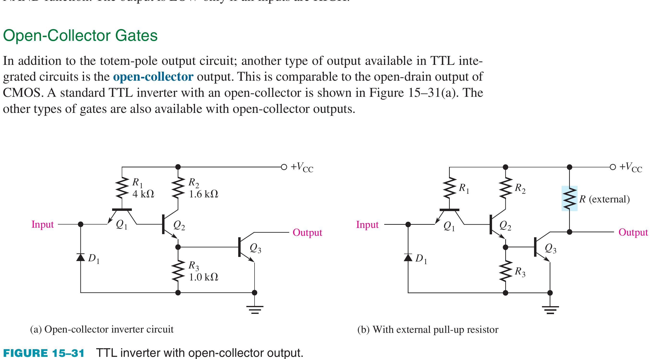
Open-collector — enables wire-AND
The pull-up transistor and level-shift diode are removed and the collector of \(Q_4\) is left open; the output is taken directly from that collector. An external pull-up resistor \(R_{ext}\) to \(V_{CC}\) is required:
- \(Q_4\) ON (saturated) → output \(\approx V_{CE(sat)} \approx 0.2\,\text{V}\) (LOW).
- \(Q_4\) OFF → no active pull-up, so \(R_{ext}\) pulls the output up to \(\approx V_{CC}\) (HIGH). Without \(R_{ext}\) the open collector would just float — the pull-up is what defines the HIGH level, and it can reach the full \(V_{CC}\) (handy for level-shifting to a higher-voltage rail).
Wire-AND. Because the pull-up is now a passive resistor, several open-collector outputs can be tied to one common node sharing a single \(R_{ext}\). If any gate's \(Q_4\) turns ON it pulls the shared node LOW (nothing actively fights it — the other side is just the resistor); the node is HIGH only when all the \(Q_4\)s are OFF. The tied node therefore realises the logical AND of all the outputs — the wired-AND — using no extra gate:
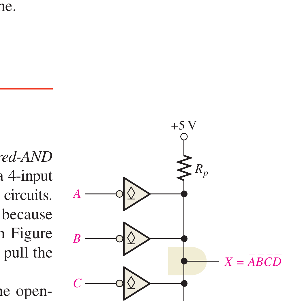
Why not just shrink \(R_{ext}\) for speed? The RC formed by \(R_{ext}\) and the load capacitance makes the LOW→HIGH edge slow, so open-collector has a larger propagation delay than totem-pole. You cannot simply make \(R_{ext}\) very small: when the output is LOW, the current through \(R_{ext}\) plus the \(I_{IL}\) of every driven input all flow into the single \(Q_4\), and if that total exceeds \(I_{OL(max)} = 16\,\text{mA}\) the transistor is damaged. This sets a lower bound on \(R_{ext}\) — which is exactly why open-collector stays slower.
Tri-state — HIGH, LOW, and high-impedance (Hi-Z)
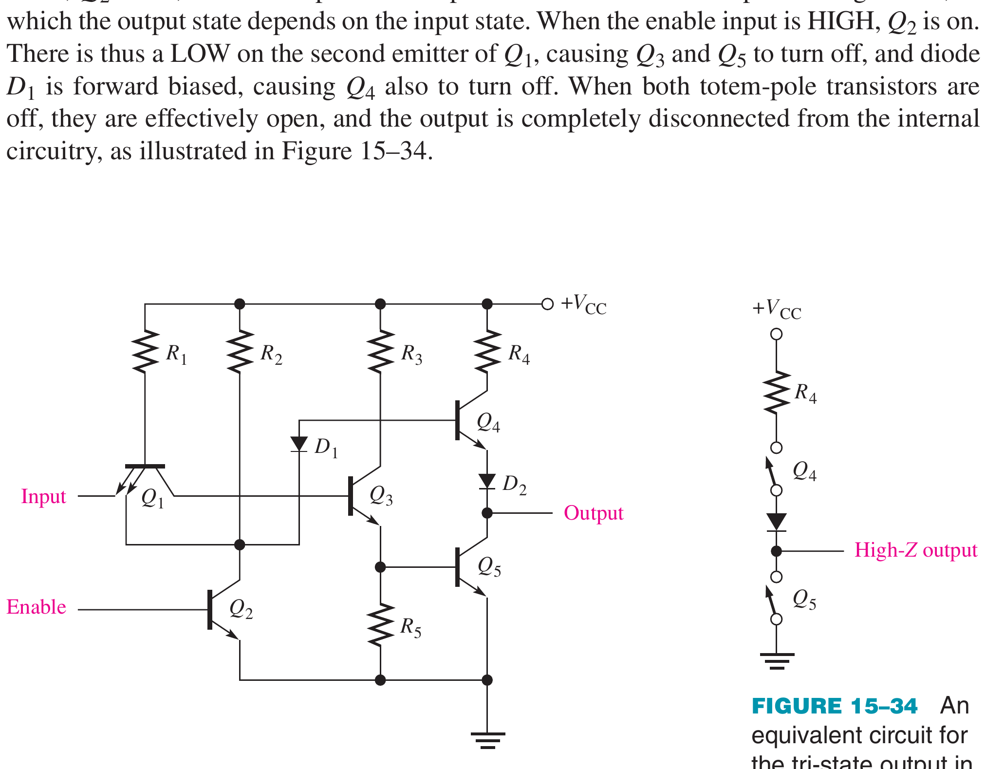
A tri-state gate adds a third output condition — high-impedance (Hi-Z) — on top of the usual HIGH and LOW, selected by an extra ENABLE control input:
- EN = 1 (enabled): the gate behaves as a normal gate (for the inverter, \(Y = \overline{A}\): input LOW → \(\approx 3.6\,\text{V}\), input HIGH → \(\approx 0.2\,\text{V}\)).
- EN = 0 (disabled): the output is disconnected from both rails — Hi-Z, neither HIGH nor LOW — so many tri-state outputs can share one common bus with only one enabled at a time.
Circuit (tri-state inverter). It is the ordinary TTL inverter with two changes: (1) the input transistor \(Q_1\) becomes multi-emitter to accept both the data input \(A\) and the enable \(EN\); (2) an extra enable diode \(D_{EN}\) is added, with its anode at the base of \(Q_3\) and its cathode at \(EN\).
- EN = 0: the \(EN\) emitter of \(Q_1\) conducts (like any LOW input) → \(Q_1\) base \(\approx 0.9\,\text{V}\), collector \(\approx 0.3\,\text{V}\) → \(Q_2\) and \(Q_4\) OFF. Simultaneously \(D_{EN}\) is forward-biased, clamping the base of \(Q_3\) to \(\approx 0.7\,\text{V}\) — below the \(\approx 1.4\,\text{V}\) needed to turn \(Q_3\) on — so \(Q_3\) is OFF too. With both output transistors off, the output floats: Hi-Z.
- EN = 1: \(D_{EN}\) is reverse-biased (its cathode is now \(\approx 5\,\text{V}\)) and drops out, and the \(EN\) emitter is off, so the circuit works as a normal inverter driven by \(A\).
TTL Sub-Families — Comparison
| Sub-Family | Propagation Delay (ns) | Power/Gate (mW) | Speed-Power Product (pJ) | Key Feature |
|---|---|---|---|---|
| 74 (Standard) | 10 | 10 | 100 | Basic TTL |
| 74L (Low Power) | 33 | 1 | 33 | Higher resistor values, less power |
| 74H (High Speed) | 6 | 22 | 132 | Lower resistor values, faster |
| 74S (Schottky) | 3 | 19 | 57 | Schottky clamp prevents deep saturation |
| 74LS (Low-Power Schottky) | 9.5 | 2 | 19 | Best TTL speed-power product |
| 74ALS (Advanced LS) | 4 | 1.2 | 4.8 | Improved LS |
| 74F (Fast) | 3 | 4 | 12 | Fastest bipolar TTL |
Speed-Power Product (in picojoules) is the figure of merit for comparing logic families: lower is better.
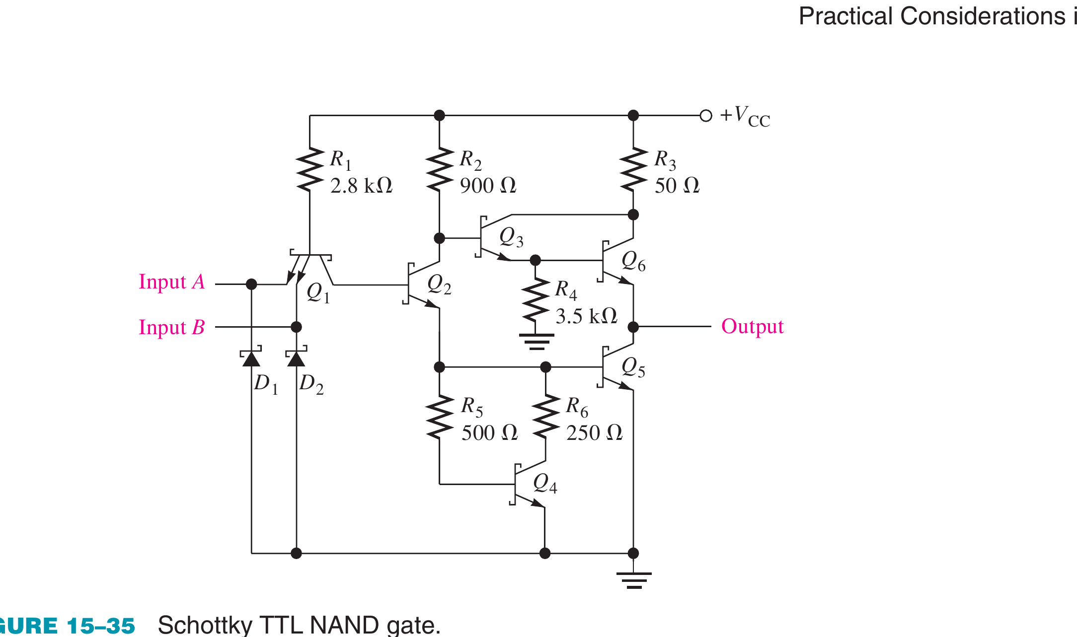
Why Schottky TTL is faster: In standard TTL, the transistors enter deep saturation, storing excess charge that must be removed during turn-off (storage time \(t_s\)). In Schottky TTL (74S, 74LS), a Schottky barrier diode (SBD) is connected across each B-C junction. Since the SBD forward voltage (\(\approx 0.3\,\text{V}\)) is less than the B-C junction forward voltage (\(\approx 0.7\,\text{V}\)), the SBD turns on first and clamps \(V_{BC}\), preventing the transistor from entering deep saturation. This virtually eliminates \(t_s\).
Key Exam Points — TTL
- TTL uses multi-emitter transistor at input and totem-pole output as standard configuration.
- In the VTC the output is HIGH (\(\approx 3.6\,\text{V}\)) for input \(< 0.8\,\text{V}\) and LOW (\(\approx 0.2\,\text{V}\)) for input \(> 2\,\text{V}\); for a HIGH input \(Q_1\) works in the reverse-active region while the totem-pole runs push–pull (only one of \(Q_3\)/\(Q_4\) conducts).
- \(V_{CC} = 5\,\text{V}\); noise margins = \(0.4\,\text{V}\) (both HIGH and LOW).
- Fan-out \(= 10\) (both states): \(I_{OL}/I_{IL} = 16/1.6\) and \(I_{OH}/I_{IH} = 400/40\).
- Totem-pole outputs cannot be wire-ANDed — two tied outputs at different levels short \(V_{CC}\!\to\!\)GND (\(Q_3\) vs \(Q_4\) fight) and can burn out. Use open-collector (passive \(R_{ext}\) pull-up) for wire-AND: \(Y = Y_1 \cdot Y_2\).
- Open-collector is slower (RC edge); \(R_{ext}\) has a lower bound set by \(I_{OL(max)} = 16\,\text{mA}\).
- Tri-state adds an ENABLE: EN = 1 → normal gate; EN = 0 → Hi-Z (both \(Q_3\) and \(Q_4\) off, the enable diode clamping \(Q_3\)'s base). Lets outputs share a bus.
- 74LS has the best speed-power product (19 pJ) among common TTL families.
- Schottky clamp eliminates storage time by preventing deep saturation.
Model Answer — TTL NAND, NOR and Inverter Operation [10 marks]
Exam-ready answer
Transistor-transistor logic (TTL) is a BJT logic family in which transistors perform both input logic and output amplification. Standard 7400 TTL uses \(V_{CC}=5\,\text{V}\) and naturally implements inverting functions.
TTL NAND structure: \(Q_1\) is a multi-emitter input transistor, one emitter per input; \(Q_2\) is a phase splitter; \(Q_3\) and diode \(D\) form the active pull-up; and \(Q_4\) is the pull-down. \(Q_3\) and \(Q_4\) form the totem-pole output.
- Any input LOW: that emitter-base junction of \(Q_1\) is forward biased and diverts current away from \(Q_2\). Hence \(Q_2\) and \(Q_4\) are OFF, while \(Q_3\) turns ON and sources current. The output is HIGH, about \(V_{CC}-V_{BE3}-V_D\approx3.6\,\text{V}\).
- All inputs HIGH: the emitter junctions are reverse biased and \(Q_1\) operates in reverse active mode; its base-collector junction feeds \(Q_2\). Then \(Q_2\) and \(Q_4\) saturate, \(Q_3\) turns OFF, and \(Y\approx V_{CE(sat)}\approx0.2\,\text{V}\).
| \(A\) | \(B\) | \(Q_2\) | \(Q_3\) pull-up | \(Q_4\) pull-down | \(Y\) |
|---|---|---|---|---|---|
| 0 | X | OFF | ON | OFF | 1 |
| X | 0 | OFF | ON | OFF | 1 |
| 1 | 1 | ON/saturated | OFF | ON/saturated | 0 |
Thus \(\boxed{Y=\overline{AB}}\). The phase splitter drives the output devices in opposite senses; the diode helps prevent both from conducting strongly together.
TTL inverter: it is the same circuit with a single-emitter \(Q_1\).
A LOW input steers current away from \(Q_2\), so \(Q_3\) raises the output; a HIGH input drives \(Q_2\) and \(Q_4\), so the output becomes LOW. Therefore \(Y=\overline A\).
TTL NOR: each input requires its own single-emitter input transistor and phase-splitter branch. The phase-splitter collectors and emitters are connected in parallel to one totem-pole stage.
- With \(A=B=0\), both splitters are OFF, \(Q_3\) is ON and \(Y=1\).
- If either input is 1, its splitter turns ON, turns \(Q_4\) ON and \(Q_3\) OFF, so \(Y=0\).
Hence \(\boxed{Y=\overline{A+B}}\). Unlike the economical multi-emitter NAND, TTL NOR duplicates an input/splitter branch for every input and therefore uses more transistors. AND and OR are obtained by following NAND and NOR respectively with an inverter.
Practical points: guaranteed standard-TTL levels are \(V_{IL}\le0.8\,\text{V}\), \(V_{IH}\ge2.0\,\text{V}\), \(V_{OL}\le0.4\,\text{V}\) and \(V_{OH}\ge2.4\,\text{V}\), giving \(NM_L=NM_H=0.4\,\text{V}\). Standard TTL is robust and fast, but saturated BJTs incur storage delay and consume static drive power; Schottky TTL prevents deep saturation to improve speed.
Practice target: 16–18 minutes; draw the NAND circuit first, explain its two input cases, then show how inverter and NOR differ.
Model Answer — TTL Output Configurations [10 marks]
Exam-ready answer
The output configuration of a TTL gate determines how it sources a HIGH, sinks a LOW, and whether several outputs may share one conductor. The three standard forms are totem-pole, open-collector and tri-state.
1. Totem-pole output: an active pull-up transistor \(Q_3\) (with level-shift diode) is stacked over pull-down \(Q_4\). The phase splitter drives them oppositely.
- HIGH: \(Q_3\) ON and \(Q_4\) OFF; the output actively sources current and rises rapidly.
- LOW: \(Q_3\) OFF and \(Q_4\) saturated; the output actively sinks current.
- Advantage: low output resistance and fast charge/discharge of load capacitance.
- Limitation: outputs cannot be tied together. If one output is HIGH while another is LOW, one pull-up fights the other pull-down and creates a destructive low-resistance path from \(V_{CC}\) to ground.
2. Open-collector output: \(Q_3\) is omitted and the collector of pull-down \(Q_4\) is brought to the output. An external resistor \(R_{ext}\) supplies the HIGH level.
- \(Q_4\) ON gives \(Y\approx V_{CE(sat)}\) (LOW).
- \(Q_4\) OFF leaves the collector open and \(R_{ext}\) raises \(Y\) to the chosen supply (HIGH).
- Several outputs may be connected: any conducting transistor pulls the node LOW, and it is HIGH only when all are OFF. In positive logic,
The pull-up and load capacitance give approximately \(\tau=R_{ext}C_L\), so the LOW-to-HIGH edge is slower than a totem-pole edge. At LOW, \(Q_4\) must sink pull-up current plus the LOW-input currents of \(N\) loads:
Hence
For \(V_{CC}=5\,\text{V}\), \(V_{OL}=0.4\,\text{V}\), \(I_{OL(max)}=16\,\text{mA}\) and four loads of \(I_{IL}=1.6\,\text{mA}\), \(R_{ext}\ge4.6/9.6\,\text{mA}\approx479\,\Omega\); a standard value at or above this limit is selected, then the HIGH-level and rise-time limits are checked. Open collector is used for wired interrupt/alarm lines and level translation.
3. Tri-state output: this retains active pull-up and pull-down but adds ENABLE. When disabled, both output transistors are OFF, producing high impedance (Hi-Z), not a third logic value.
| Enable | Data action | Output |
|---|---|---|
| 1 | Gate operates normally | 0 or 1 |
| 0 | Pull-up and pull-down both OFF | Hi-Z |
Many tri-state outputs can share a bidirectional data bus, provided control logic enables only one driver at a time; otherwise bus contention occurs. Unlike open collector, an enabled tri-state gate actively drives both levels and therefore switches quickly, but it cannot provide wired-AND logic.
| Feature | Totem-pole | Open collector | Tri-state |
|---|---|---|---|
| HIGH drive | Active | Passive \(R_{ext}\) | Active when enabled |
| Shared connection | No | Yes, wired-AND | Yes, one enabled at a time |
| Special state | None | Floating without pull-up | Controlled Hi-Z |
| Main use | Ordinary fast logic | Shared request/level shift | Buses and multiplexed lines |
Practice target: 16–18 minutes; draw all three stages, derive wired-AND and the pull-up constraint, and distinguish floating from controlled Hi-Z.