Analog-to-Digital Conversion
Possible Exam Questions
Exam Questions and Answer Map
Evidence note: [PYQ paper/year] = exact question observed in that past paper; [likely] = pattern-predicted variant not confirmed as an exact PYQ.
- State the sampling theorem. Explain aliasing and the methods used to prevent it. [5] — [likely]
- Answer plan: State \(f_s\geq2f_m\) -> define Nyquist rate and Nyquist frequency -> explain spectral overlap -> draw correct/undersampled spectra -> state anti-alias LPF, guard band and oversampling.
-
Model answer: Sampling, Aliasing and Prevention
-
Explain the sampling theorem and describe A-law and \(\mu\)-law companding. [5] — [PYQ 2082]
- Answer plan: State the theorem and aliasing condition -> define companding -> write both laws and parameters -> compare regions and low-level performance -> state why speech PCM needs nonuniform quantization.
-
Model answer: Sampling Theorem and Companding
-
Explain a sample-and-hold circuit, its operation and important specifications. Why is it required before an ADC? [5] — [likely]
- Answer plan: Draw switch-capacitor-buffer circuit -> describe sample and hold modes -> explain finite ADC conversion time -> define acquisition time, aperture uncertainty, droop, hold step and feedthrough.
-
Model answer: Sample-and-Hold before an ADC
-
Explain quantization error and derive \(SQNR_{dB}\approx6.02n+1.76\) for a full-scale sinusoid. [10] — [likely]
- Answer plan: Define \(L=2^n\) and \(\Delta=V_{FS}/2^n\) -> bound error by \(\pm\Delta/2\) -> integrate uniform error to get \(\Delta^2/12\) -> divide full-scale sine power by noise power -> convert to dB.
-
Model answer: Quantization Error and SQNR Derivation
-
Explain the principle of A/D conversion. With a neat diagram, describe a successive-approximation ADC. [3+7=10] — [PYQ Eng. Sewa]
- Answer plan: State sampling/holding/comparison/encoding principle [3] -> draw SAR register, DAC and comparator [7] -> explain MSB-to-LSB binary search -> state fixed \(n\)-cycle conversion time and uses.
-
Model answer: Principle and Successive-Approximation ADC
-
Compare flash, counter, SAR, dual-slope and sigma-delta ADCs. [10] — [likely]
- Answer plan: Give each block principle -> compare speed, resolution, conversion time, hardware, noise rejection and applications -> identify flash as fastest, SAR as general purpose, dual-slope as precision and sigma-delta as high-resolution low-bandwidth.
-
Model answer: ADC Architecture Comparison
-
Explain binary-weighted, R-2R ladder and current-steering DACs and state important DAC specifications. [10] — [likely]
- Answer plan: State ideal DAC relation -> explain weighted currents, ladder halving and switched current sources -> compare resistor matching, speed and integration -> define resolution, settling time, accuracy, INL, DNL and monotonicity.
- Model answer: DAC Architectures and Specifications
1. Conversion Overview
Natural sources such as speech, temperature and light produce analog signals. A digital system represents these signals using a sequence of finite-length binary words.
Analog-to-Digital Chain

| Stage | Purpose |
|---|---|
| Anti-aliasing LPF | Restrict input bandwidth before sampling |
| Sampler / sample-and-hold | Measure the signal at discrete instants and keep it steady |
| Quantizer | Map each sample to one of a finite number of levels |
| Encoder | Assign an \(n\)-bit codeword to the selected level |
Sampling discretizes time, quantization discretizes amplitude, and encoding represents the quantized level in binary.
Digital-to-Analog Chain
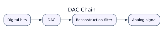
A DAC converts each input code to a voltage or current. A reconstruction low-pass filter removes switching images and smooths the staircase or pulse output.
2. Sampling Theorem
Statement
If a continuous-time signal is strictly band-limited to a highest frequency \(f_m\), it can be reconstructed exactly from uniformly spaced samples if:
where \(f_s\) is the sampling frequency.
| Term | Definition |
|---|---|
| Nyquist rate | Minimum sampling rate for a signal of bandwidth \(f_m\): \(2f_m\) |
| Nyquist frequency | Highest unaliased baseband frequency at a given \(f_s\): \(f_s/2\) |
| Sampling period | \(T_s=1/f_s\) |
Equality is the ideal theoretical limit. A practical converter uses \(f_s>2f_m\) so a realizable anti-aliasing filter has a transition band.
Frequency-Domain Explanation
Uniform sampling replicates the message spectrum around integer multiples of \(f_s\). If adjacent replicas do not overlap, an ideal reconstruction LPF can recover the original baseband spectrum.
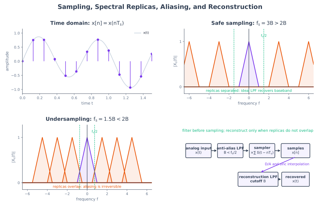
Aliasing
Aliasing is the irreversible overlap of spectral replicas caused by sampling a signal outside the permitted Nyquist band. A sinusoid at input frequency \(f_{in}\) may appear after sampling at an alias frequency:
where integer \(k\) is chosen so \(0\leq f_a\leq f_s/2\).
Once two analog frequencies produce the same sample sequence, no digital filter can separate them.
Prevention of Aliasing
- Place an analog anti-aliasing LPF before the sampler.
- Set its passband to include the wanted signal and attenuate components above \(f_s/2\).
- Use a sampling rate above the theoretical Nyquist rate.
- Leave a guard band for practical filter roll-off.
Oversampling and Undersampling
- Oversampling: \(f_s\) is much greater than \(2f_m\). It relaxes the analog filter, spreads quantization noise over a wider spectrum and enables digital decimation.
- Accidental undersampling: a baseband signal violates \(f_s\geq2f_m\) and aliases destructively.
- Intentional bandpass sampling: a narrow RF band may be sampled below twice its highest carrier frequency if a valid bandpass-sampling condition is met and a sharp preselector prevents other bands from folding into it. This is not permission to violate the Nyquist condition for arbitrary baseband signals.
Practical Example
Telephone speech is limited to approximately \(3.4\,\text{kHz}\):
Standard telephony uses \(8\,\text{kHz}\), giving a \(4\,\text{kHz}\) Nyquist frequency and a transition band between \(3.4\) and \(4\,\text{kHz}\).
3. Sampling Methods
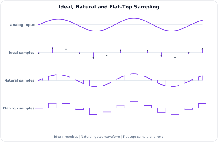
Ideal or Impulse Sampling
The signal is multiplied by an impulse train:
The sample values are exact, but zero-width impulses are a mathematical model rather than a realizable circuit.
Natural Sampling
The signal is gated by finite-width pulses. During each gate opening, the pulse top follows the analog input. Natural sampling is realizable with an analog switch, but the varying pulse top is inconvenient for many ADCs.
Flat-Top Sampling
A sample-and-hold circuit captures the input and maintains one constant value over the aperture. It is the practical ADC waveform. Finite hold width gives a sinc-shaped frequency response called the aperture effect, which can be compensated when necessary.
| Sampling type | Pulse top | Practical status | Main issue |
|---|---|---|---|
| Ideal | Zero-width impulse | Mathematical model | Not physically realizable |
| Natural | Follows input during gate | Realizable | ADC input is still changing |
| Flat-top | Constant held value | Standard ADC method | Aperture droop / sinc distortion |
4. Sample-and-Hold Circuit
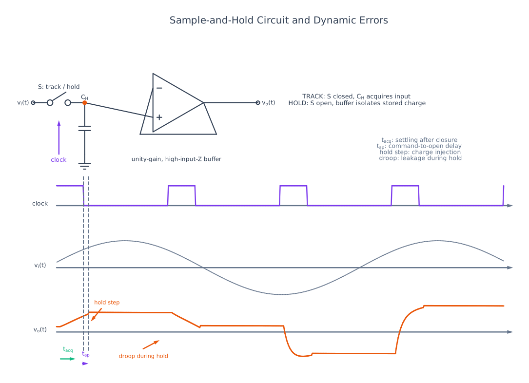
A sample-and-hold (S/H) circuit captures the input voltage at a selected instant and holds it approximately constant while the ADC completes conversion.
Operation
| Mode | Switch | Capacitor | Output |
|---|---|---|---|
| Sample / track | Closed | Charges toward input through switch resistance | Follows \(v_i(t)\) |
| Hold | Open | Retains stored charge | Remains near sampled value |
The output buffer has high input impedance, so it draws little charge from \(C_H\), and low output impedance, so it can drive the ADC.
Why It Is Required
An ADC takes finite time to compare and encode its input. If the input changes significantly during that interval, different internal bit decisions correspond to different input values. Holding the input eliminates this dynamic conversion error.
Important Specifications
| Specification | Meaning |
|---|---|
| Acquisition time | Time after switch closure needed to settle within the required error band |
| Aperture delay | Delay from sampling command to actual disconnection |
| Aperture jitter | Uncertainty in the sampling instant; especially important at high input frequency |
| Droop rate | Rate at which held voltage changes because of leakage |
| Hold step / pedestal | Output jump caused by switch charge injection when hold begins |
| Feedthrough | Unwanted coupling of input or clock to output during hold |
| Settling accuracy | Error band reached before conversion begins |
For a sinusoidal input, aperture jitter \(\sigma_t\) imposes an approximate SNR limit:
5. Quantization
Quantization maps every held sample to the nearest member of a finite set of amplitude levels.
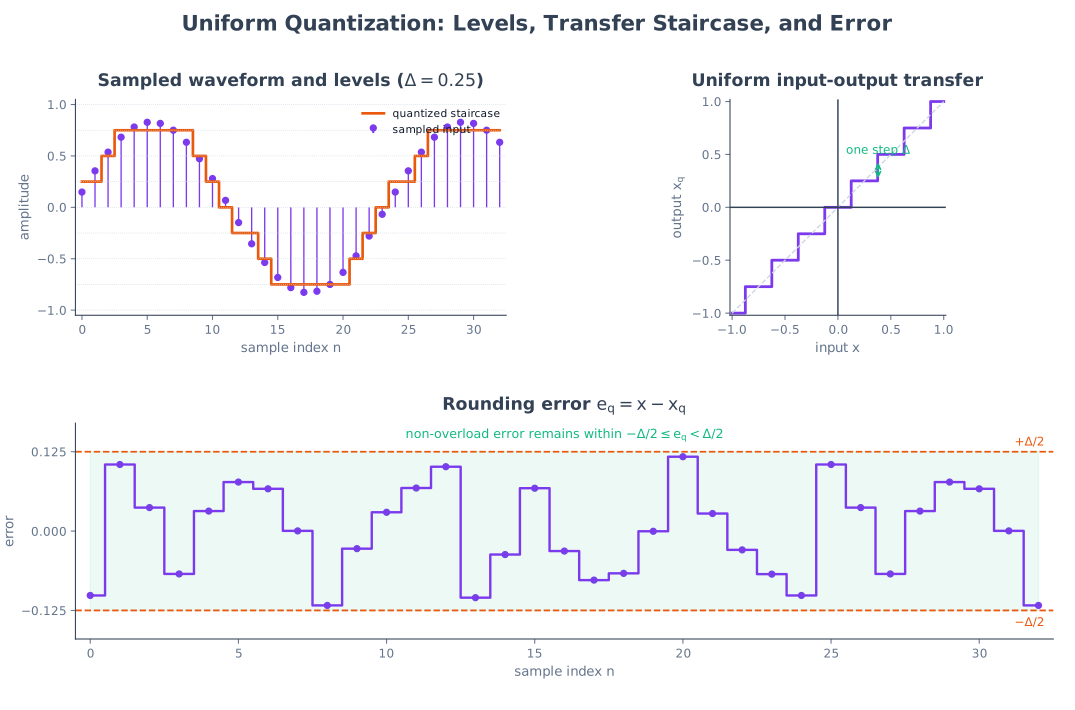
Levels and Resolution
For an ideal \(n\)-bit converter:
For full-scale input span \(V_{FS}\), the ideal least-significant-bit step is commonly taken as:
Some data sheets define endpoint spacing as \(V_{FS}/(2^n-1)\); use the convention stated in the question.
Quantization Error
For rounding to the nearest level:
If the error is modeled as uniformly distributed and uncorrelated with a sufficiently active input, its mean-square value is:
SQNR Derivation for a Full-Scale Sinusoid
For a bipolar range \(-V_p\) to \(+V_p\):
Signal power for \(x(t)=V_p\sin\omega t\) is:
Quantization-noise power is:
Therefore:
Converting to decibels:
This formula assumes an ideal quantizer and a full-scale sinusoidal input. Smaller signals have lower SQNR in a uniform quantizer.
Uniform and Nonuniform Quantization
| Feature | Uniform | Nonuniform |
|---|---|---|
| Step size | Constant | Small near zero, larger at high amplitude |
| Circuit concept | Direct uniform ADC | Compressor + uniform ADC, or variable thresholds |
| Weak-signal SQNR | Poorer | Better |
| Main use | General measurement | Speech PCM |
6. Companding
Companding combines compression at the transmitter with complementary expansion at the receiver. It approximates nonuniform quantization while using a uniform quantizer internally.
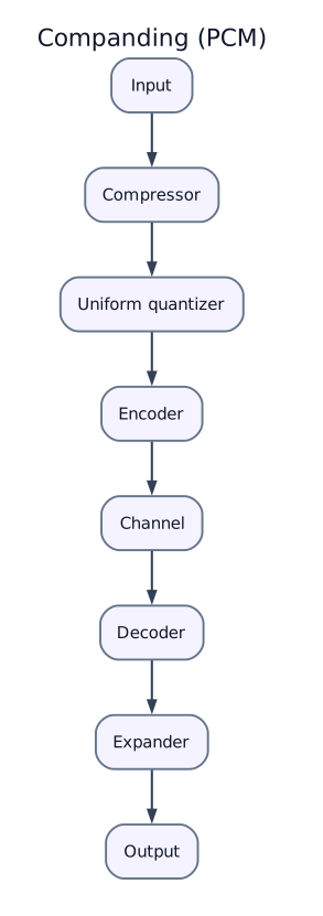
Speech spends much of its time at low amplitudes. Compression expands the relative spacing of weak samples before quantization, reducing their fractional quantization error.
\(\mu\)-Law
For normalized \(|x|\leq1\):
The standard parameter is:
It is used mainly in North American and Japanese PCM systems.
A-Law
For normalized \(|x|\leq1\):
The standard parameter is:
It is used in European and many international E1 systems.
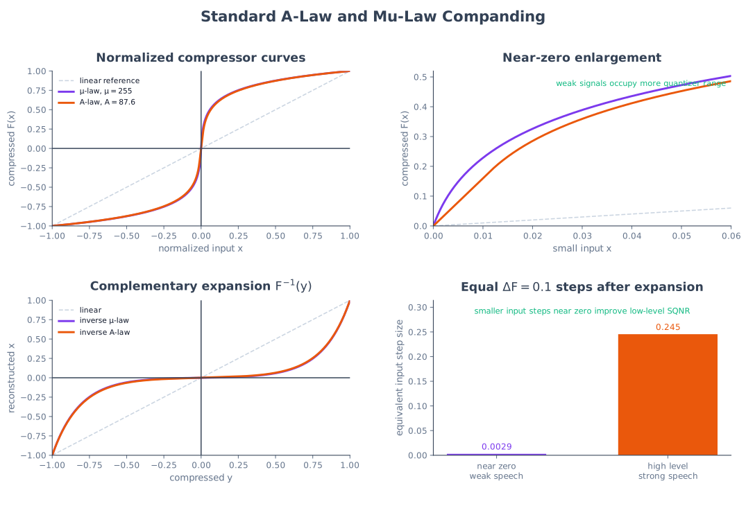
Comparison
| Feature | A-law | \(\mu\)-law |
|---|---|---|
| Parameter | \(A=87.6\) | \(\mu=255\) |
| Common region | Europe/international | North America/Japan |
| Piecewise-linear approximation | 13-segment characteristic | 15-segment characteristic |
| Small-signal compression | Slightly less | Slightly greater |
| Purpose | Improve low-level speech SQNR | Improve low-level speech SQNR |
The exact improvement depends on input level and implementation; companding does not remove quantization noise.
7. ADC Principle and Specifications
An ADC compares a held analog value with one or more reference levels and encodes the result as a digital word.
Ideal Transfer Relation
For a unipolar ideal ADC:
with saturation at the minimum and maximum codes.
Core Specifications
| Specification | Meaning |
|---|---|
| Resolution | One LSB or \(1/2^n\) of full-scale span |
| Conversion time | Time from conversion start to valid output |
| Throughput / sampling rate | Maximum complete conversions per second |
| Offset error | Horizontal shift of actual transfer curve |
| Gain error | Full-scale slope error after offset removal |
| DNL | Difference between actual and ideal code-bin width |
| INL | Maximum deviation from an ideal straight transfer line |
| Missing code | An output code never produced for any input |
| SNR / SINAD | Noise-only or noise-plus-distortion performance |
| ENOB | Effective resolution derived from measured SINAD |
For a sinusoidal test:
8. ADC Architectures
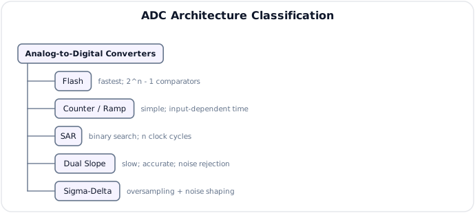
Flash ADC
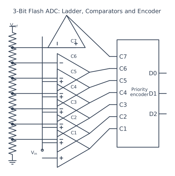
An \(n\)-bit flash ADC uses a resistor ladder, \(2^n-1\) comparators and a priority encoder.
- The ladder creates all decision thresholds.
- Every comparator compares \(V_{in}\) simultaneously with one threshold.
- The comparator outputs form a thermometer code.
- A priority encoder produces the binary output.
Advantages: fastest architecture and one comparison interval.
Limitations: comparator count, input capacitance, power and cost grow exponentially. An 8-bit flash ADC needs \(255\) comparators.
Applications: oscilloscopes, radar, direct RF/IF sampling and high-speed data acquisition.
Counter or Digital-Ramp ADC
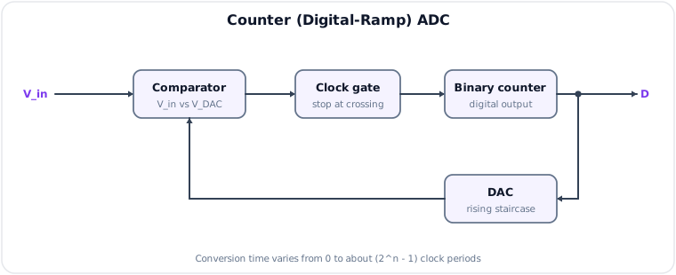
- A counter starts from zero and drives a DAC.
- A comparator checks the DAC output against \(V_{in}\).
- Counting stops when \(V_{DAC}\geq V_{in}\).
- The counter state is the digital result.
Worst-case conversion requires approximately \(2^n-1\) clock periods, and conversion time depends on input amplitude. The architecture is simple but slow.
Successive-Approximation (SAR) ADC
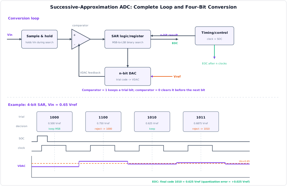
A SAR ADC performs a binary search:
- The sample-and-hold freezes \(V_{in}\).
- The SAR tentatively sets the MSB to 1 and all lower bits to 0.
- The DAC converts that trial code to \(V_{DAC}\).
- If \(V_{DAC}\leq V_{in}\), the bit is retained; otherwise it is cleared.
- The next bit is tested in the same way down to the LSB.
- After \(n\) decisions, the register contains the final code.
An ideal \(n\)-bit SAR ADC takes a fixed \(n\) comparison cycles, independent of input amplitude. It offers a strong speed-resolution-power balance and is common in microcontrollers and instrumentation.
Dual-Slope ADC
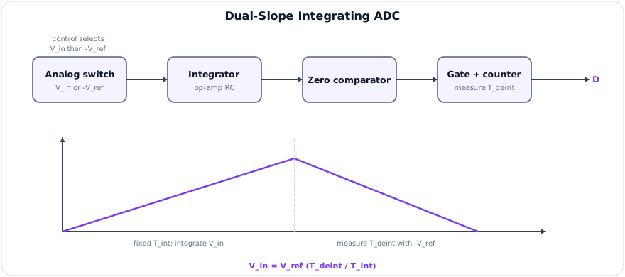
A dual-slope converter has two integration phases:
- Integrate unknown \(V_{in}\) for a fixed interval \(T_{int}\).
- Apply an opposite-polarity precision reference \(V_{ref}\).
- Count the time \(T_{deint}\) required for the integrator output to return to zero.
Charge balance gives:
The result depends mainly on time and reference accuracy, not on the absolute \(RC\) product. Integrating over a whole number of mains periods gives excellent \(50/60\,\text{Hz}\) noise rejection. The architecture is slow and is widely used in digital multimeters.
Sigma-Delta ADC
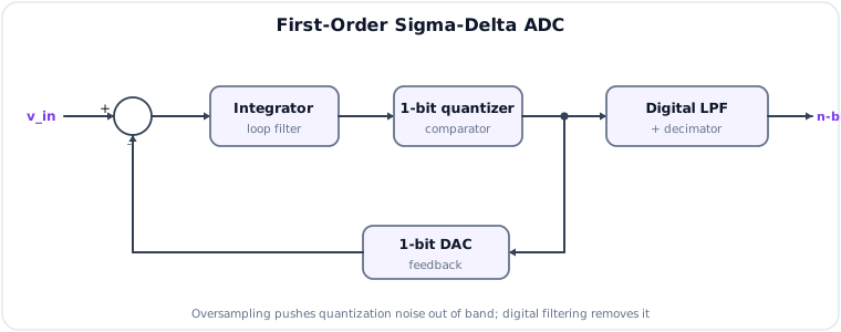
A sigma-delta ADC uses:
- Oversampling far above the signal Nyquist rate.
- A feedback loop that forces average one-bit DAC output to track the input.
- Noise shaping, which moves much quantization noise to high frequencies.
- A digital low-pass and decimation filter that removes out-of-band noise and reduces sample rate.
It provides very high resolution for audio, sensors and precision measurement, but has latency and is not the first choice for very wide instantaneous bandwidth.
ADC Comparison
| Type | Speed | Conversion time | Typical resolution | Main strength | Main application |
|---|---|---|---|---|---|
| Flash | Very high | Fixed, shortest | Low to medium | Maximum speed | Oscilloscope, RF data acquisition |
| Counter | Low | Input-dependent | Medium | Simplicity | Low-cost control |
| SAR | Medium to high | Fixed, about \(n\) cycles | Medium to high | Balanced performance | MCU, instrumentation |
| Dual slope | Low | Fixed integration + variable deintegration | High | Accuracy and mains rejection | Digital multimeter |
| Sigma-delta | Low to medium signal bandwidth | Filter-dependent latency | Very high | Resolution and noise performance | Audio, sensor, precision ADC |
9. Digital-to-Analog Converters (DAC)
Principle
An ideal unipolar \(n\)-bit DAC converts unsigned code \(D\) to:
The maximum code \(D=2^n-1\) therefore produces one LSB less than \(V_{ref}\) under this convention.
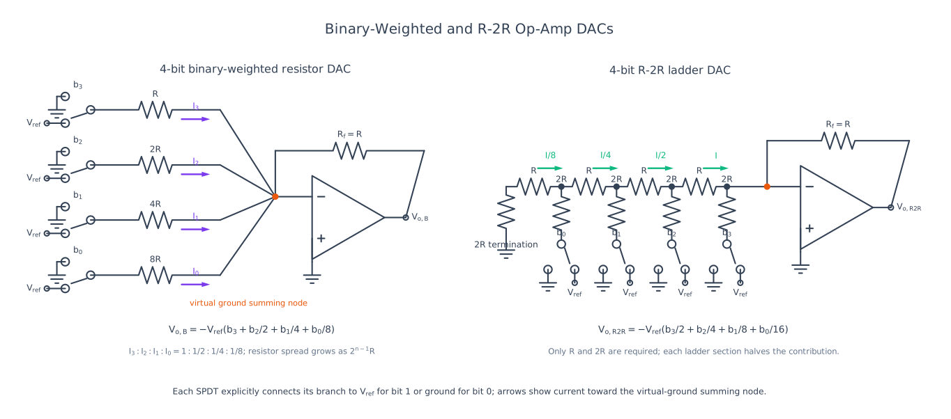
Binary-Weighted Resistor DAC
Each bit controls a branch weighted by \(R,2R,4R,\ldots,2^{n-1}R\). An op-amp sums the branch currents.
Advantages: direct concept and fast conversion.
Limitations: requires a very wide range of accurately ratioed resistors and switch resistances, so high resolution is difficult.
R-2R Ladder DAC
The ladder uses only two resistor values, \(R\) and \(2R\). At each node the network divides current by two, producing binary weighting without exponentially large resistor values.
Advantages:
- Easier matching and IC fabrication.
- Constant resistance environment for switches.
- Practical for higher resolution than a simple binary-weighted network.
Current-Steering DAC
Matched current sources represent binary or segmented weights. High-speed switches steer each source either to the output summing node or to a dummy node.
Advantages: very fast and suitable for communication waveform generation.
Limitations: sensitive to current-source mismatch, switching glitches and output compliance. High-resolution designs often use thermometer coding for MSBs and binary weighting for LSBs.
DAC Specifications
| Specification | Meaning |
|---|---|
| Resolution | Smallest ideal output change, one LSB |
| Settling time | Time after a code change to enter and remain within an error band |
| Accuracy | Closeness of actual output to ideal output |
| Offset error | Output error at zero code |
| Gain error | Slope/full-scale error after offset removal |
| DNL | Error in individual code-step size |
| INL | Deviation from ideal transfer line |
| Monotonicity | Output never reverses direction when code increases |
| Glitch impulse | Transient output energy during code transitions |
For monotonic operation without missing steps, a common sufficient condition is \(DNL>-1\,\text{LSB}\) for every code transition.
10. Key Exam Points
Key Exam Points - Analog-to-Digital Conversion
- Sampling theorem: \(f_s\geq2f_m\); practical systems use a guard band and anti-aliasing LPF.
- Ideal, natural and flat-top sampling differ in pulse shape; ADCs use sample-and-hold flat tops.
- Quantization levels: \(L=2^n\); ideal step: \(\Delta=V_{FS}/2^n\).
- Rounding error is bounded by \(\pm\Delta/2\) and has modeled power \(\Delta^2/12\).
- Ideal full-scale-sine SQNR is \(6.02n+1.76\,\text{dB}\).
- Companding implements nonuniform speech quantization: A-law uses \(A=87.6\) and \(\mu\)-law uses \(\mu=255\).
- Flash is fastest; SAR takes about \(n\) decisions; dual slope is precise but slow; sigma-delta uses oversampling and noise shaping.
- An R-2R DAC needs only two resistor values; current steering is preferred for very high speed.
- Resolution is not the same as accuracy. Offset, gain, INL, DNL, noise and settling also matter.
Model Answer — Sampling, Aliasing and Prevention [5 marks]
Exam-ready answer
The sampling theorem states that a continuous-time signal strictly band-limited to a highest frequency \(f_m\) hertz can be reconstructed uniquely from uniform samples if
\(2f_m\) is the Nyquist rate of that signal, whereas \(f_s/2\) is the Nyquist frequency for a chosen sampler. Equality is an ideal limit; a practical system chooses \(f_s>2f_m\) to leave a transition band for a realizable filter.
Sampling by an impulse train produces shifted spectral replicas:
If \(f_s\geq2f_m\), adjacent replicas do not overlap and a reconstruction low-pass filter can select the baseband copy. If the condition is violated, replicas overlap and different analog frequencies produce the same samples. This irreversible folding is aliasing.
An input sinusoid then appears in the first Nyquist zone at
For example, sampling \(f_{in}=5.5\,\text{kHz}\) at \(f_s=8\,\text{kHz}\) gives the false component \(f_a=|5.5-8|=2.5\,\text{kHz}\).
Prevention: place an analog anti-alias low-pass filter before the sampler, limit its passband to the wanted \(f_m\), attenuate all components that could fold below \(f_s/2\), sample above the theoretical minimum, and provide a guard band for filter roll-off. Oversampling relaxes the analog filter and permits digital filtering/decimation, but it does not rescue frequencies already aliased at the sampling instant. A practical sample-and-hold then keeps each accepted sample constant during conversion; its finite aperture gives a sinc-like high-frequency droop and aperture jitter limits high-frequency SNR.
Practice target: 8–9 minutes; state both Nyquist terms, draw the separated/overlapped replicas, calculate one alias, and list the prevention chain.
Model Answer — Sampling Theorem and Companding [5 marks, PYQ 2082]
Exam-ready answer
For a message strictly limited to \(|f|\leq f_m\), uniform sampling permits exact ideal reconstruction when
Sampling repeats \(X(f)\) around \(0,\pm f_s,\pm2f_s,\ldots\). When \(f_s<2f_m\), adjacent copies overlap and high-frequency content folds into the baseband; this is aliasing and cannot be removed digitally. Therefore the practical chain is analog anti-alias LPF \(\rightarrow\) sample-and-hold \(\rightarrow\) quantizer, with \(f_s\) chosen above \(2f_m\) to provide a guard band.
Companding means compression before a uniform quantizer and complementary expansion after decoding. Speech contains many weak samples, so a logarithmic compressor gives small input amplitudes relatively larger code spacing and improves their quantization SQNR; the expander restores the original amplitude law. It approximates nonuniform quantization without requiring a nonuniform binary ADC.
For normalized \(|x|\leq1\), the standard \(\mu\)-law characteristic is
It is used mainly in North America and Japan. The standard A-law characteristic is
and is common in European/international E1 telephony. A-law is linear very near zero and logarithmic above \(1/A\); \(\mu\)-law is logarithmic in one expression and gives somewhat stronger small-signal compression. Both improve low-level speech performance at the expense of deliberately nonuniform error versus input level; neither eliminates quantization noise. As a check, a \(3.4\,\text{kHz}\) telephone channel needs at least \(6.8\,\text{kHz}\) sampling, and the standard \(8\,\text{kHz}\) rate leaves a practical filter transition band.
Practice target: 9 minutes; reserve about 2 marks for sampling/aliasing and 3 marks for the companding chain, both laws, constants and regional use.
Model Answer — Sample-and-Hold before an ADC [5 marks]
Exam-ready answer
A sample-and-hold (S/H) circuit captures the instantaneous analog input voltage and presents an approximately constant value to an ADC during its finite conversion interval. Its basic blocks are an analog switch, hold capacitor \(C_H\), high-input-impedance buffer and a sampling clock.
During sample/track mode, the clock closes the switch and \(C_H\) charges toward \(v_i(t)\) through the source and switch resistance; the buffered output follows the input. The acquisition time is the interval required to settle within the specified fraction of an LSB. At the sampling command the switch opens. During hold mode, the capacitor retains the captured charge and the buffer isolates it from the ADC load, so \(v_o\approx v_i(t_s)\) until conversion ends.
The circuit is necessary because comparator, SAR or integrating decisions take nonzero time. Without holding, the input could move while different bits are being decided, so one output word would correspond to several input values. The permitted input change is commonly kept below a fraction of one LSB, where \(1\,\text{LSB}=V_{FS}/2^n\).
Important specifications are: acquisition time; aperture delay, from command to actual disconnection; aperture jitter \(\sigma_t\), the uncertainty of that instant; droop rate, caused by leakage during hold; hold step/pedestal, caused by switch charge injection; feedthrough, unwanted input or clock coupling while held; and settling accuracy. For a sinusoidal input, timing uncertainty imposes approximately
For example, \(f_{in}=100\,\text{kHz}\) and \(\sigma_t=10\,\text{ps}\) give about \(104\,\text{dB}\); increasing input frequency by a factor of ten reduces this limit by \(20\,\text{dB}\). Flat-top holding also has an aperture sinc response, so aperture width and droop become important at high frequency or high resolution.
Practice target: 8–9 minutes; draw the switch-capacitor-buffer path, explain both clock states, and define at least five dynamic specifications.
Model Answer — Quantization Error and Full-Scale-Sine SQNR [10 marks]
Exam-ready answer
Quantization replaces every held sample by the nearest one of a finite number of amplitude levels. For an ideal \(n\)-bit uniform quantizer spanning \(V_{FS}\),
The encoder then assigns an \(n\)-bit word to the selected level. Sampling discretizes time; quantization discretizes amplitude.
Let \(x_q\) be the rounded level and \(e_q=x-x_q\). Except at overload, nearest-level rounding gives
For a sufficiently active input whose error samples can be modeled as uniformly distributed and uncorrelated over this interval, the mean error is zero and the mean-square noise is
Now take a full-scale bipolar sinusoid \(x(t)=V_p\sin\omega t\) over the range \(-V_p\) to \(+V_p\). Then \(V_{FS}=2V_p\) and
Hence
Converting the power ratio to decibels,
so
Thus every added bit ideally improves full-scale-sine SQNR by about \(6\,\text{dB}\). For \(n=8\), \(L=256\) and \(SQNR\approx49.92\,\text{dB}\). If \(V_{FS}=2\,\text{V}\), then \(\Delta=2/256=7.8125\,\text{mV}\) and the maximum rounding error is \(3.906\,\text{mV}\).
The result assumes an ideal uniform quantizer, no clipping, negligible thermal/jitter/nonlinearity noise, a full-scale sine, and a sufficiently decorrelated error. A sine below full scale has the same nominal step but less signal power, so its SQNR falls by the back-off in dB. Very small or periodic inputs can make error signal-dependent rather than white. Overload produces clipping error outside the \(\pm\Delta/2\) model. Nonuniform quantization or A/\(\mu\)-law companding improves weak-speech SQNR by using finer effective steps near zero, but does not change the stated ideal full-scale uniform result.
Practice target: 17–18 minutes; show the error integral, substitute the bipolar full-scale step, preserve power units, and finish with assumptions plus the 8-bit check.
Model Answer — Principle and Successive-Approximation ADC [10 marks, Eng. Sewa PYQ]
Exam-ready answer
Part A — Principle of A/D conversion [3 marks]
An ADC converts a band-limited analog quantity into a finite binary word. The anti-alias filter first restricts input bandwidth; a sampler/S&H takes values at \(f_s\geq2f_m\) and keeps each value steady; the quantizer compares it with reference thresholds and chooses one of \(L=2^n\) levels; the encoder outputs the corresponding \(n\)-bit code. For span \(V_{FS}\),
for ideal nearest-level rounding. Resolution alone does not guarantee accuracy; reference, offset, gain, INL, DNL, noise and timing also matter.
Part B — Successive-approximation conversion [7 marks]
A SAR ADC uses one comparator, an \(n\)-bit DAC and a successive-approximation register to perform an MSB-to-LSB binary search on a held input.
- A start-of-conversion (SOC) command freezes \(V_{in}\) in the S/H and clears/initializes the SAR.
- The SAR tentatively sets the MSB, producing trial code \(100\ldots0\). The DAC generates \(V_{DAC}=V_{ref}/2\).
- The comparator decides whether the trial is above or below \(V_{in}\). Retain the bit if \(V_{DAC}\leq V_{in}\); otherwise clear it.
- Set the next bit provisionally, while keeping previous decisions, and compare again.
- Continue to the LSB. After \(n\) comparisons the SAR latches the code and asserts end-of-conversion (EOC).
For straight binary weighting,
Four-bit example: let \(V_{ref}=16\,\text{V}\) and held \(V_{in}=10.4\,\text{V}\), so one LSB is \(1\,\text{V}\).
| Trial code | \(V_{DAC}\) | Comparator decision |
|---|---|---|
| 1000 | \(8\,\text{V}\) | Keep MSB |
| 1100 | \(12\,\text{V}\) | Clear \(b_2\) |
| 1010 | \(10\,\text{V}\) | Keep \(b_1\) |
| 1011 | \(11\,\text{V}\) | Clear \(b_0\) |
The final result is \(1010_2=10\), representing \(10\,\text{V}\) under this DAC convention. The search takes a fixed \(n\) decision clocks, independent of input magnitude, unlike a counter ADC whose delay may approach \(2^n-1\) clocks.
SAR offers a useful speed-resolution-power compromise and is common in microcontrollers, sensor interfaces and data acquisition. Its limitations are DAC settling and linearity, comparator offset/noise, reference error, capacitor/resistor matching and S/H acquisition/aperture error. The input must remain within the allowed error band for the complete search.
Practice target: 16–18 minutes; spend about 5 minutes on the 3-mark conversion chain and 11–13 minutes on the labeled SAR loop, trial table, fixed timing, merits and limits.
Model Answer — Flash, Counter, SAR, Dual-Slope and Sigma-Delta ADCs [10 marks]
Exam-ready answer
All ADCs assign a held input to one of \(2^n\) codes, but their method of finding the code determines speed, hardware, noise rejection and resolution.
Flash ADC: a resistor string creates \(2^n-1\) thresholds. The same number of parallel comparators produce a thermometer code in one comparison interval, and a priority encoder converts it to binary. It is the fastest type, but area, power, input capacitance and offset-matching burden grow exponentially. For example, 8 bits require \(255\) comparators. It suits oscilloscopes, radar and very wideband acquisition.
Counter/digital-ramp ADC: a clocked binary counter drives a DAC. A comparator stops the count when \(V_{DAC}\geq V_{in}\); the count is the result. Hardware is simple, but conversion time depends on input and ranges from about one to \(2^n-1\) clocks. It is too slow for rapidly changing signals unless an S/H is used.
SAR ADC: one comparator, feedback DAC and SAR test trial codes from MSB to LSB. Each comparison halves the remaining range, so an \(n\)-bit result requires approximately \(n\) fixed decision cycles. It offers medium/high speed, moderate power and commonly medium/high resolution, making it the general-purpose choice for embedded and instrumentation work.
Dual-slope ADC: an integrator first integrates unknown \(V_{in}\) for fixed \(T_{int}\), then an opposite reference is applied until the output returns to zero. Charge balance gives
for consistent polarity magnitudes. The shared \(RC\) scale cancels, and selecting \(T_{int}\) as an integer number of mains periods strongly rejects \(50/60\,\text{Hz}\) interference. It is precise but slow, so it is used in digital multimeters and precision DC measurement.
Sigma-delta ADC: a subtractor, integrator, usually one-bit quantizer and one-bit feedback DAC run at a high oversampling rate. The loop noise-shapes quantization error toward high frequencies; a digital low-pass/decimation filter removes it and reduces sample rate. With \(OSR=f_s/(2B)\) it achieves very high resolution and linearity for audio/sensors, but has digital-filter latency and limited instantaneous signal bandwidth.
| Type | Code-search operation | Conversion time | Hardware / resolution trend | Noise behavior | Typical use |
|---|---|---|---|---|---|
| Flash | All thresholds in parallel | Shortest, fixed | \(2^n-1\) comparators; low/medium resolution | Captures instantaneous noise | RF, video, oscilloscope |
| Counter | Count upward through DAC levels | Variable, up to \(2^n-1\) clocks | Very simple; modest speed | Little inherent rejection | Low-cost control |
| SAR | Binary search | Fixed, about \(n\) clocks | Balanced speed/power; medium/high resolution | Moderate | MCU, DAQ, instrumentation |
| Dual slope | Integrate then timed de-integrate | Long | Precision rather than speed | Excellent averaging/mains rejection | DMM, weighing |
| Sigma-delta | Oversampled feedback plus decimation | Filter-dependent latency | Very high narrowband resolution | Shapes noise out of band | Audio, sensors |
As a scale comparison, a 12-bit flash would need \(4095\) comparators; a 12-bit SAR needs about 12 comparisons; a counter may need 4095 clocks; a dual-slope may deliberately integrate for thousands of clocks; and sigma-delta trades a very high internal sample rate for a much lower, accurately filtered output rate. Therefore “fastest” is flash, “balanced general purpose” is SAR, “best integrating precision” is dual-slope, and “highest narrowband resolution” is sigma-delta, subject to actual converter specifications.
Practice target: 18–20 minutes; give each conversion path and timing law, then reproduce the five-row comparison and one hardware-count example.
Model Answer — Binary-Weighted, R-2R and Current-Steering DACs [10 marks]
Exam-ready answer
A DAC maps an \(n\)-bit code \(D\) to a proportional analog voltage or current. Under one ideal unipolar convention,
so one ideal step is \(V_{ref}/2^n\) and full-scale code is one LSB below \(V_{ref}\). A zero-order-hold DAC output contains steps and switching images; a reconstruction low-pass filter recovers the wanted smooth waveform.
Binary-weighted resistor DAC: each bit switch connects a branch to \(V_{ref}\) or ground. Branch resistors \(R,2R,4R,\ldots,2^{n-1}R\) produce currents weighted \(1,1/2,1/4,\ldots\), and an op-amp sums them. For an inverting four-bit design with feedback \(R_f=R\),
up to the circuit's chosen scaling. It is direct and fast, but high resolution requires a very wide range of precisely ratioed resistors and negligible switch resistance.
R-2R ladder DAC: every section uses only \(R\) and \(2R\). Looking into each ladder node gives the same equivalent resistance, so current divides by two successively and creates binary weights. Switches steer each bit to reference or ground and an op-amp sums the ladder output. Only a 2:1 resistor ratio must match, making IC fabrication, scaling and switch loading better than the simple weighted network; finite matching still limits INL/DNL.
Current-steering DAC: matched unit or binary/segmented current sources are always on, while high-speed switches steer their currents to the output or a dummy node. A transimpedance/load converts total current to voltage. Thermometer-coded MSBs reduce major-carry glitches, while binary LSBs limit area. It is the fastest common DAC form for RF and waveform generation, but source mismatch, output compliance, clock skew and switching transients limit accuracy and spectral purity.
| Property | Binary weighted | R-2R ladder | Current steering |
|---|---|---|---|
| Weight creation | Many resistor values | Repeated \(R\) and \(2R\) division | Matched switched currents |
| Integration | Difficult at high \(n\) | Good | Excellent but area/current costly |
| Speed | High | High | Very high |
| Main limitation | Resistor range and switch resistance | Ratio matching and settling | Source mismatch, glitch, compliance |
| Typical use | Low-resolution teaching/simple DAC | General voltage DAC | Video, RF, direct synthesis |
Important specifications are: resolution, one LSB; accuracy, total closeness to ideal; offset error, output at zero code; gain error, slope/full-scale error after offset removal; DNL, actual step minus one ideal LSB; INL, deviation from the ideal transfer line; monotonicity, output never decreases as code increases; settling time, time after a code change to enter and remain inside a stated error band; glitch impulse, transient energy during unequal switch timing; and output noise/temperature drift. \(DNL>-1\,\text{LSB}\) is a common sufficient monotonicity condition.
Example: for an ideal 8-bit, \(V_{ref}=5.12\,\text{V}\) DAC, one LSB is \(5.12/256=20\,\text{mV}\). Code \(D=160\) gives \(V_o=5.12(160/256)=3.20\,\text{V}\). A real result must also be checked against INL, DNL, gain, settling and load specifications; nominal resolution alone is not accuracy.
Practice target: 18–20 minutes; draw the two resistor networks, explain current steering, state the ideal transfer/example, and define at least eight specifications.