Push-Pull Power Amplifiers
Possible Exam Questions
Exam Questions and Answer Map
-
Explain Class-B push-pull operation with circuit diagrams and derive its maximum efficiency. [10] — [likely]
-
Answer plan: State need → distinguish transformer and complementary forms → trace positive/negative paths → derive \(P_L\), \(P_{DC}\) and \(\eta_{max}\) → discuss dissipation, merits, limitations and uses.
-
Model answer: Class-B Push-Pull Operation and Efficiency
-
What is crossover distortion? Explain Class-AB bias and thermal stabilisation. [5] — [likely]
-
Answer plan: Define \(V_{BE}\) dead zone → show zero-crossing notch → apply about \(2V_{BE}\) → explain thermal tracking, emitter resistors and correct quiescent-current setting.
- Model answer: Crossover Distortion, Class AB and Thermal Stability
1. Definition and Need
A push-pull amplifier uses two active devices so that their output contributions have opposite current directions and combine in the load. In Class B, one device handles the positive half-cycle and the other the negative half-cycle.
Push-pull operation is used because it:
- delivers both halves of a high-power waveform;
- gives much higher ideal efficiency than Class A;
- ideally draws no quiescent Class-B output current;
- can cancel even-order distortion and DC magnetisation in a symmetric transformer primary;
- permits impedance matching or transformerless complementary output.
2. Class A, B and AB Bias
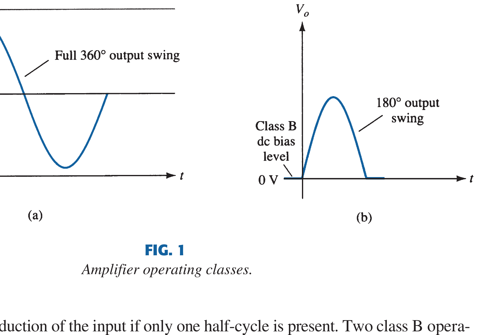
| Class | Bias and conduction per device | Idle current | Main result |
|---|---|---|---|
| A | Well inside active region; \(360^\circ\) | High | Best linearity; low efficiency |
| B | At cutoff; \(180^\circ\) | Ideally zero | High efficiency; crossover dead zone |
| AB | Slightly above cutoff; \(>180^\circ\) | Small | Overlap removes most crossover distortion |
Push-pull can be Class A, but Class B/AB is normally chosen for output power. Class-AB efficiency is signal-dependent: it lies between corresponding Class-A and Class-B behaviour and approaches the Class-B limit at large output; it is not a fixed \(50\)–\(78.5\%\) for every signal level.
3. Complementary-Symmetry Class B
Complementary symmetry uses matched NPN/PNP BJTs (or NMOS/PMOS devices) in emitter/source-follower form and does not require an output transformer.
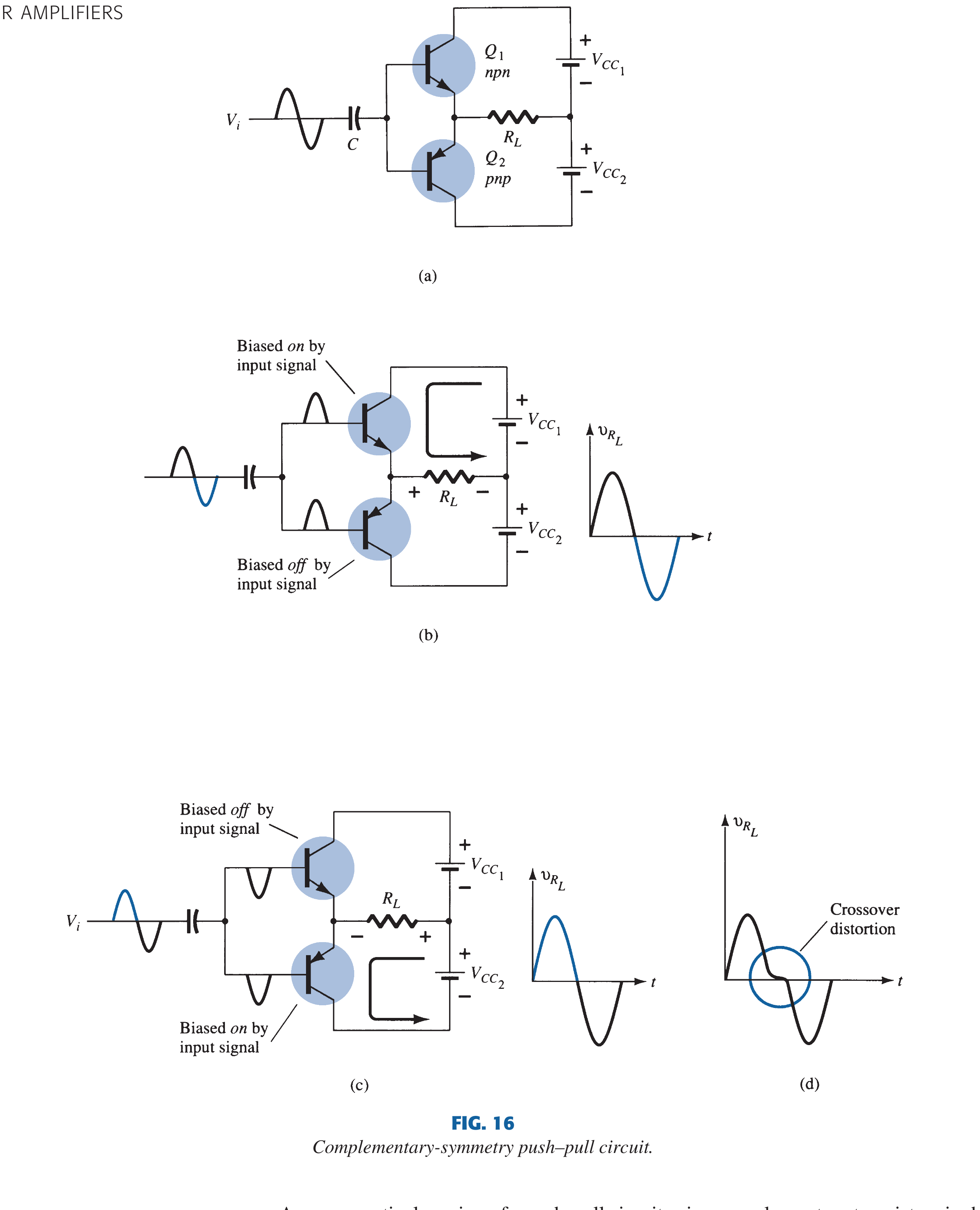
Positive Half-Cycle
- NPN \(Q_N\) is forward biased and sources load current.
- PNP \(Q_P\) is off.
- The output follows the positive input excursion, less device headroom.
Negative Half-Cycle
- PNP \(Q_P\) is forward biased and sinks load current toward the negative rail.
- NPN \(Q_N\) is off.
- The output follows the negative excursion.
The load receives the reconstructed full cycle. “Complementary” refers to opposite-polarity devices with corresponding characteristics; “symmetry” means the two paths should behave as nearly alike as practical.
4. Transformer-Coupled Class B
Two same-polarity transistors may instead be driven \(180^\circ\) apart by a centre-tapped input transformer. Their collector currents flow in alternate halves of a centre-tapped output-transformer primary; the secondary combines the flux changes and drives \(R_L\).
Transformer vs Complementary Form
| Property | Transformer-coupled | Complementary-symmetry |
|---|---|---|
| Output devices | Same polarity possible | Complementary pair required |
| Phase splitting | Input transformer | Drive circuit/device polarity |
| Load matching | Excellent by turns ratio | No inherent matching |
| DC in load | Blocked by transformer | Usually direct/capacitor coupled |
| Size and bandwidth | Bulky; core/leakage limits | Compact; broad audio response |
| Modern use | Special matching/RF/legacy power | Common audio and IC output stages |
5. Class-B Power and Efficiency
For an ideal complementary stage with symmetric \(\pm V_{CC}\) rails,
The load power is
Each rail supplies a half-wave current with average \(I_p/\pi\), so total DC input power is
Therefore
At the ideal maximum \(V_p=V_{CC}\),
Practical swing and efficiency are lower because of saturation/dropout voltage, bias current, driver loss, finite transistor gain and load/transformer loss.
6. Device Heat Dissipation
Total output-device dissipation is
For symmetric devices, average dissipation per transistor is
Differentiating with respect to \(V_p\) shows maximum per-device dissipation occurs at
This is below full output. A heat sink must therefore be designed for the worst device dissipation, not merely the maximum load power point.
7. Crossover Distortion
A silicon BJT needs roughly \(0.6\)–\(0.7\,\text{V}\) \(V_{BE}\) for substantial conduction. Around zero input,
neither ideal Class-B device conducts. The output develops a notch/dead band at every zero crossing, producing especially objectionable odd harmonics at small signal level.
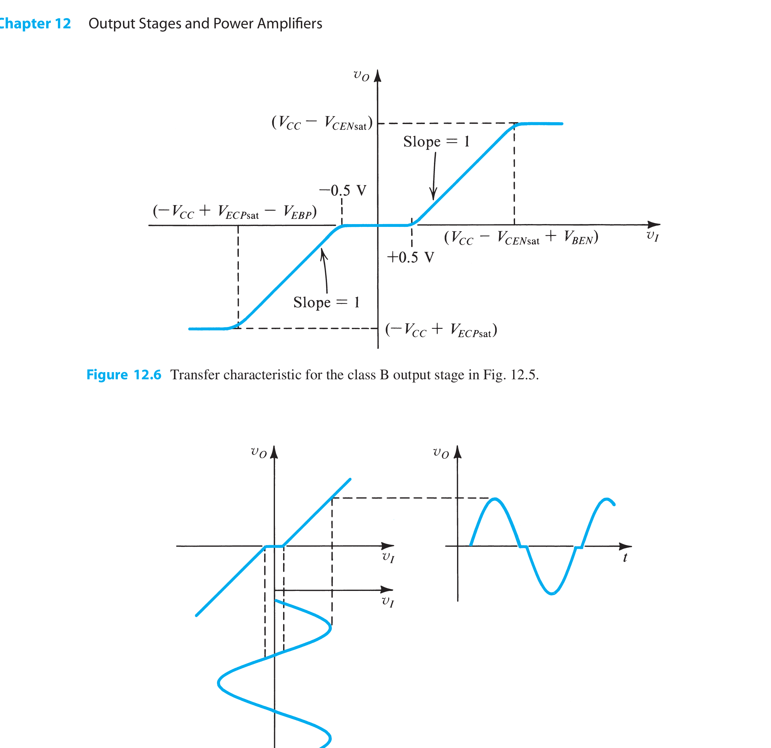

Book-grounded distortion test
The Class-B transfer curve is approximately flat for \(-V_{BE}<v_i<+V_{BE}\), so a small sinusoid loses output around every zero crossing. Class-AB bias shifts both device characteristics toward overlap, replacing the dead band with a small quiescent current. Draw the transfer curve and waveform notch together for a strong 5-mark explanation.
Source figure: Sedra/Smith, Microelectronic Circuits (7th ed.), PDF p. 959.
8. Class-AB Remedy and Thermal Stability
Apply approximately \(2V_{BE}\) between complementary bases using two forward-biased diodes or an adjustable \(V_{BE}\) multiplier. Both devices then carry a small quiescent current and their transfer curves overlap.
Thermal design is essential because BJT \(V_{BE}\) falls by roughly \(2\,\text{mV}/^\circ\text{C}\) at a given current. Heating can otherwise raise current, causing more heating and possible thermal runaway.
Practical controls are:
- thermally couple bias diodes/\(V_{BE}\) multiplier to the output devices;
- use small emitter resistors for local current feedback and sharing;
- set and verify quiescent current after warm-up;
- provide an adequate heat sink and, where needed, current/temperature protection.
Too little bias leaves crossover distortion; too much causes excessive idle dissipation or simultaneous-conduction (shoot-through) current.
9. Advantages, Disadvantages and Applications
Advantages
- high ideal Class-B efficiency;
- little ideal no-signal dissipation;
- large AC load power;
- even-harmonic and supply-ripple cancellation when paths are symmetric;
- complementary form needs no output transformer.
Disadvantages
- Class B has crossover distortion;
- Class AB needs accurate, thermally tracked bias;
- matched complementary devices and driver current may be required;
- transformer form is bulky, costly and bandwidth-limited;
- short-circuit and thermal protection are important at power level.
Applications
Audio power amplifiers, loudspeaker/headphone drivers, servo and actuator drivers, RF linear stages (with suitable tuned/load networks) and transmitter power stages.
Exam Traps
- \(78.5\%\) is the ideal maximum, not typical practical efficiency.
- Maximum transistor dissipation does not occur at maximum output power.
- Class AB reduces crossover distortion but introduces quiescent dissipation.
- “Push” and “pull” describe alternating load-current directions, not voltage amplification alone.
Rapid Recall
- Positive half: upper/NPN path conducts.
- Negative half: lower/PNP or second transformer-driven path conducts.
- \(P_L=V_p^2/(2R_L)\).
- \(P_{DC}=2V_{CC}V_p/(\pi R_L)\).
- \(\eta_{max}=\pi/4\).
- Cure crossover with thermally tracked Class-AB bias.
Model Answer — Class-B Push-Pull Operation and Efficiency [10 marks]
Exam-ready answer
A Class-B push-pull amplifier uses two devices biased at cutoff, each conducting for \(180^\circ\). One supplies the positive load-current half-cycle and the other supplies the negative half-cycle. This uses supply power more efficiently than Class A and reconstructs a full load waveform.
In complementary symmetry, positive input forward-biases the NPN, which sources current through \(R_L\), while the PNP is off. Negative input forward-biases the PNP, which sinks current, while the NPN is off. In transformer coupling, a centre-tapped input secondary drives two same-polarity transistors in antiphase; alternate collector currents excite opposite halves of a centre-tapped output primary and the secondary combines them.
For symmetric \(\pm V_{CC}\) supplies and sinusoidal output peak \(V_p\),
Each supply carries a half-wave current whose average is \(I_p/\pi\), hence
Therefore
The ideal maximum load power is \(V_{CC}^2/(2R_L)\). Device dissipation is \(P_{DC}-P_L\); per transistor it is maximised at \(V_p=2V_{CC}/\pi\), where \(P_{D(max)}=V_{CC}^2/(\pi^2R_L)\), not at full output.
Advantages are high efficiency, low ideal idle loss, large output and cancellation in a symmetric pair. Limitations are crossover distortion, thermal/bias control, device matching and protection; transformers additionally add bulk, loss and restricted bandwidth. Uses include audio, servo and transmitter power stages.
Practice target: 18 minutes; draw one complementary and one transformer form, trace both half-cycles, derive \(P_L\), \(P_{DC}\) and \(\pi/4\), then state the dissipation trap.
Model Answer — Crossover Distortion, Class AB and Thermal Stability [5 marks]
Exam-ready answer
Crossover distortion is the zero-crossing notch in an unbiased complementary Class-B stage. A silicon transistor needs about \(0.6\)–\(0.7\,\text{V}\) \(V_{BE}\), so for approximately \(-V_{BE}<v_i<+V_{BE}\) neither output transistor carries appreciable current. The load voltage becomes flat or discontinuous near zero and gains odd harmonics.
Class AB applies approximately \(2V_{BE}\) between the bases with two forward diodes or a \(V_{BE}\) multiplier. A small quiescent current then keeps both devices just conducting at zero, and each conducts slightly more than \(180^\circ\) so their transfer curves overlap.
Bias must track temperature. As a BJT heats, \(V_{BE}\) falls, which can increase current and cause thermal runaway. Bias diodes or the \(V_{BE}\) multiplier are thermally coupled to the output devices; emitter resistors add current feedback and aid sharing; a heat sink and current/temperature protection remove and limit heat. Too little bias leaves a notch, while too much causes high idle loss or shoot-through.
Practice target: 8 minutes; draw the dead zone and two-diode remedy, then state the too-little/too-much-bias consequences and three thermal controls.