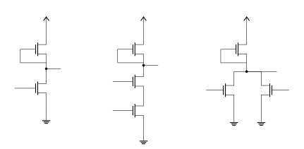
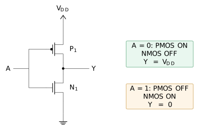
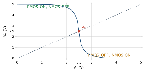
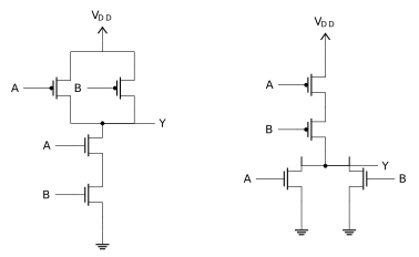
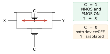
Fig: Depletion-load NMOS inverter Y= A, NAND Y=AB with a series PDN, and NOR Y=A+B with a parallel PDN. Each load has its gate tied to source and is always conductingFig: CMOS inverter and its two stable current-path statesFig: Representative CMOS inverter VTC. The dashed line locates V_I=V_O; its intersection gives the switching point V_MFig: Complementary two-input CMOS networks: NAND uses a parallel PMOS PUN and series NMOS PDN; NOR uses a series PMOS PUN and parallel NMOS PDNFig: CMOS transmission gate with complementary control