A/D Converters
Possible Exam Questions
Exam Questions and Answer Map
Questions marked [PYQ paper/year] were directly observed in past papers; [likely] means pattern-based prediction, not a claimed past question. Rehearse each answer plan closed-book, then check the full answer via the links.
-
Explain successive-approximation A/D conversion with a block diagram. [3+7=10] — [PYQ Eng. Sewa]
-
Answer plan: Define sampling, quantisation and resolution → draw S/H, comparator, SAR and DAC → explain the MSB-to-LSB binary search → state the fixed \(n\)-clock conversion time.
-
Model answer: Successive-Approximation A/D Conversion
-
Compare flash, SAR and dual-slope ADCs. [10] — [likely]
-
Answer plan: Compare architecture, conversion time, resolution, hardware, noise rejection and applications.
-
Model answer: Flash, SAR and Dual-Slope ADC Comparison
-
Explain sigma-delta conversion and the roles of oversampling and noise shaping. [5] — [likely]
-
Answer plan: Define oversampling ratio → explain the one-bit quantiser/DAC loop → show noise moved out of band → explain digital decimation.
- Model answer: Sigma-Delta Conversion, Oversampling and Noise Shaping
1. Analog-to-Digital (A/D) Converters
Likely Exam Question (10 marks)
"Explain the working of a successive approximation ADC with a block diagram and timing diagram." OR "Compare flash, successive approximation, and dual-slope ADC."
Definition
An Analog-to-Digital Converter (ADC) converts a continuous analog signal (voltage) into a discrete digital representation (binary number). The key parameters are:
- Resolution (\(n\) bits): The number of output bits. An \(n\)-bit ADC divides the input range into \(2^n\) levels.
- Quantization step (LSB): \(\Delta = V_{ref} / 2^n\) — the smallest detectable change.
- Conversion time: Time required to complete one conversion.
- Sampling rate: Maximum number of conversions per second.
Flash (Parallel) ADC
Definition: A flash ADC is the fastest type of ADC. It uses \(2^n - 1\) comparators in parallel, each with a different reference voltage set by a resistor ladder. All comparators operate simultaneously — the input voltage is compared against all reference levels at once, and a priority encoder converts the comparator outputs (thermometer code) to an \(n\)-bit binary output.
Block diagram components:
- Resistor ladder: \(2^n\) equal resistors divide \(V_{ref}\) into \(2^n - 1\) reference levels.
- \(2^n - 1\) comparators: Each compares \(V_{in}\) with its reference level.
- Priority encoder: Converts thermometer code to binary.
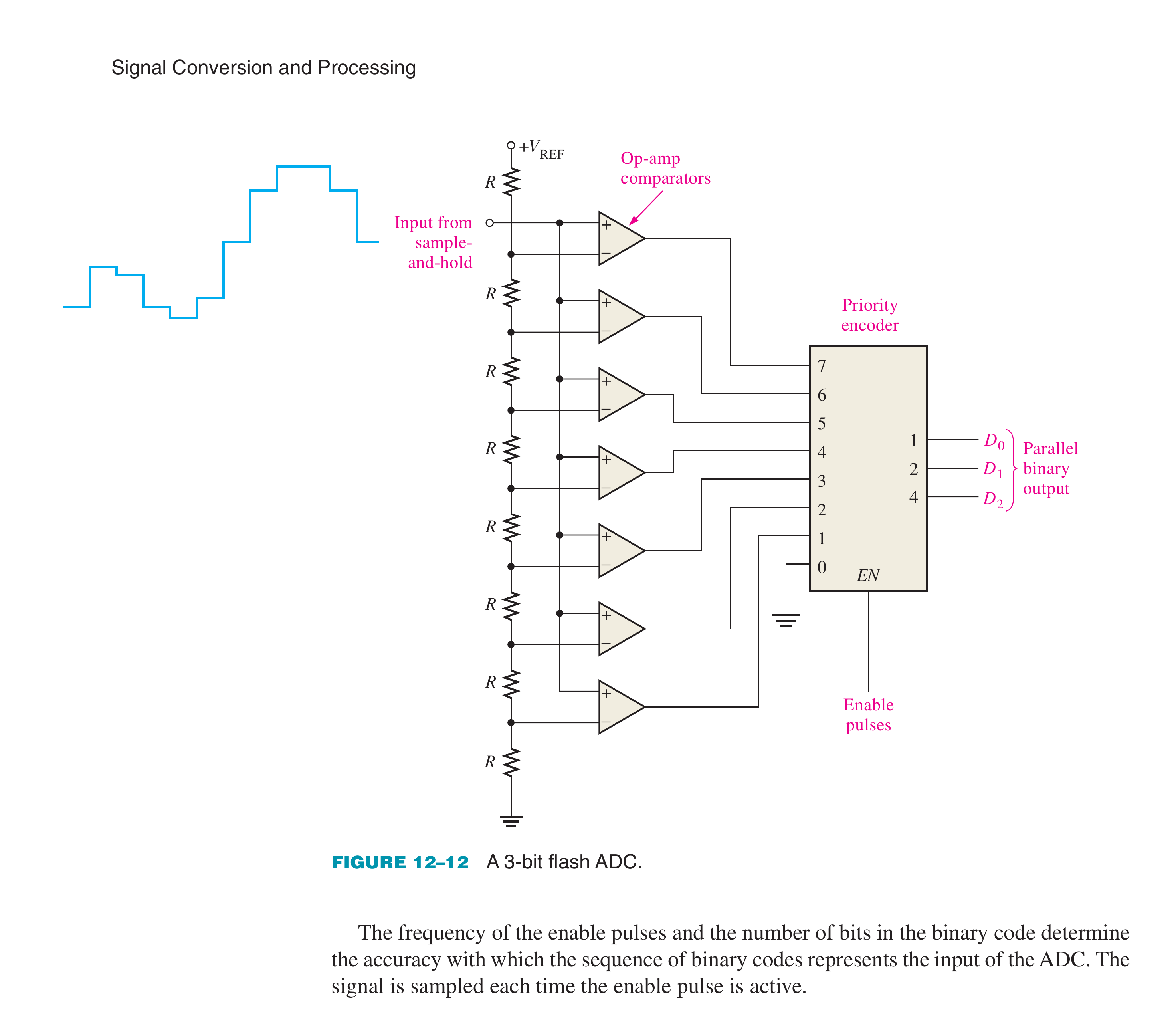

Book-grounded flash-ADC count
An \(n\)-bit flash converter resolves \(2^n\) codes using \(2^n-1\) thresholds and comparators. All comparisons occur in parallel; the encoder converts the resulting thermometer code to binary. This explains both its one-step speed and its exponential area/power cost.
Source figure: Floyd, Digital Fundamentals (11th ed.), PDF p. 707.
Characteristics:
- Fastest ADC — conversion in one clock cycle.
- Resolution limited by number of comparators: \(n\)-bit ADC needs \(2^n - 1\) comparators.
- Exponential hardware growth: 8-bit → 255 comparators, 10-bit → 1023 comparators.
- Power consumption and cost increase rapidly with resolution.
- Practical for low to medium resolution (up to ~8 bits).
Applications: Video digitization, oscilloscopes, radar, high-speed data acquisition (where speed is critical and resolution can be moderate).
Successive Approximation ADC (SAR ADC)
Definition: A successive approximation ADC (SAR ADC) uses a binary search algorithm to converge on the digital output. Starting from the MSB, it tests each bit one at a time by setting it to 1, comparing the resulting DAC output with the input voltage, and keeping or clearing the bit based on the comparison result.
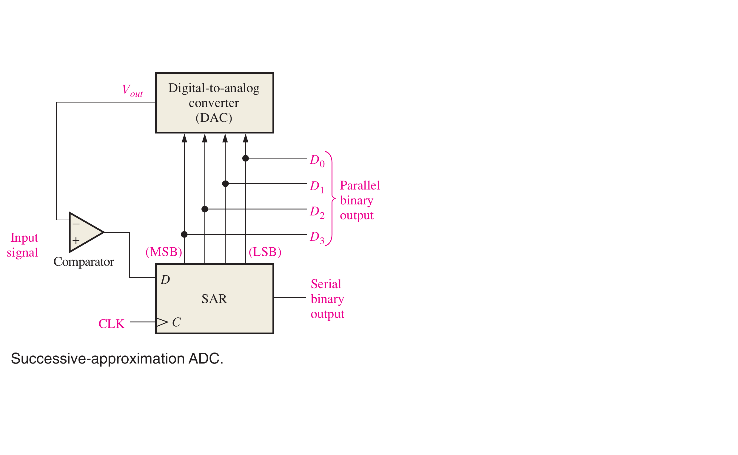
Book-grounded SAR timing
After acquisition, an ideal \(n\)-bit SAR makes one comparator decision per bit, from MSB to LSB, so conversion takes a fixed \(n\) trial clocks (plus acquisition/control overhead), independent of the input value. The held input must not move by more than the allowed conversion error during those trials.
Source figure: Floyd, Digital Fundamentals (11th ed.), PDF p. 710.
Block diagram components:
- Sample-and-hold (S/H): Captures the analog input and holds it constant during conversion.
- Successive Approximation Register (SAR): Controls the binary search — sets/clears bits based on comparator output.
- DAC (Digital-to-Analog Converter): Converts the SAR's current digital estimate to an analog voltage.
- Comparator: Compares DAC output with \(V_{in}\).
- Clock and control logic.
Algorithm (for an \(n\)-bit conversion):
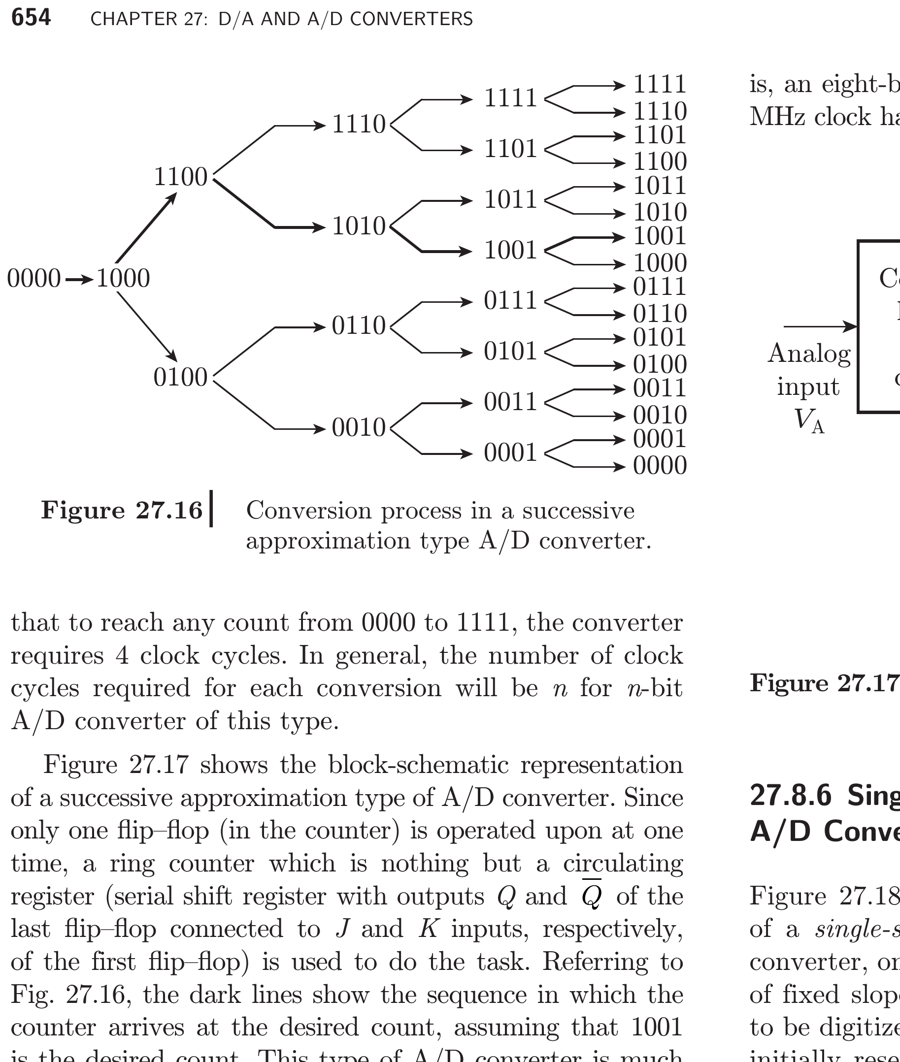
- Set MSB (\(b_{n-1}\)) = 1, all others = 0. DAC output = \(V_{ref}/2\).
- Compare: If \(V_{in} \geq V_{DAC}\), keep MSB = 1. Else, clear MSB = 0.
- Set next bit (\(b_{n-2}\)) = 1.
- Compare again and decide.
- Repeat for all bits from MSB to LSB.
- After \(n\) clock cycles, conversion is complete.
Characteristics:
- Conversion time = \(n\) clock cycles (fixed, independent of input).
- Good balance of speed and resolution.
- Moderate hardware complexity.
- Most popular ADC architecture for medium speed, medium-to-high resolution (8–18 bits).
Applications: Data acquisition systems, digital multimeters, sensor interfaces, embedded systems.
Dual-Slope (Integrating) ADC
Definition: A dual-slope ADC measures the input voltage by integrating it for a fixed time period, then integrating a known reference voltage in the opposite direction until the integrator output returns to zero. The time for the second integration is proportional to the input voltage.
Block diagram components:
- Integrator (op-amp + capacitor)
- Comparator (detects zero crossing)
- Counter (measures time)
- Control logic and switches
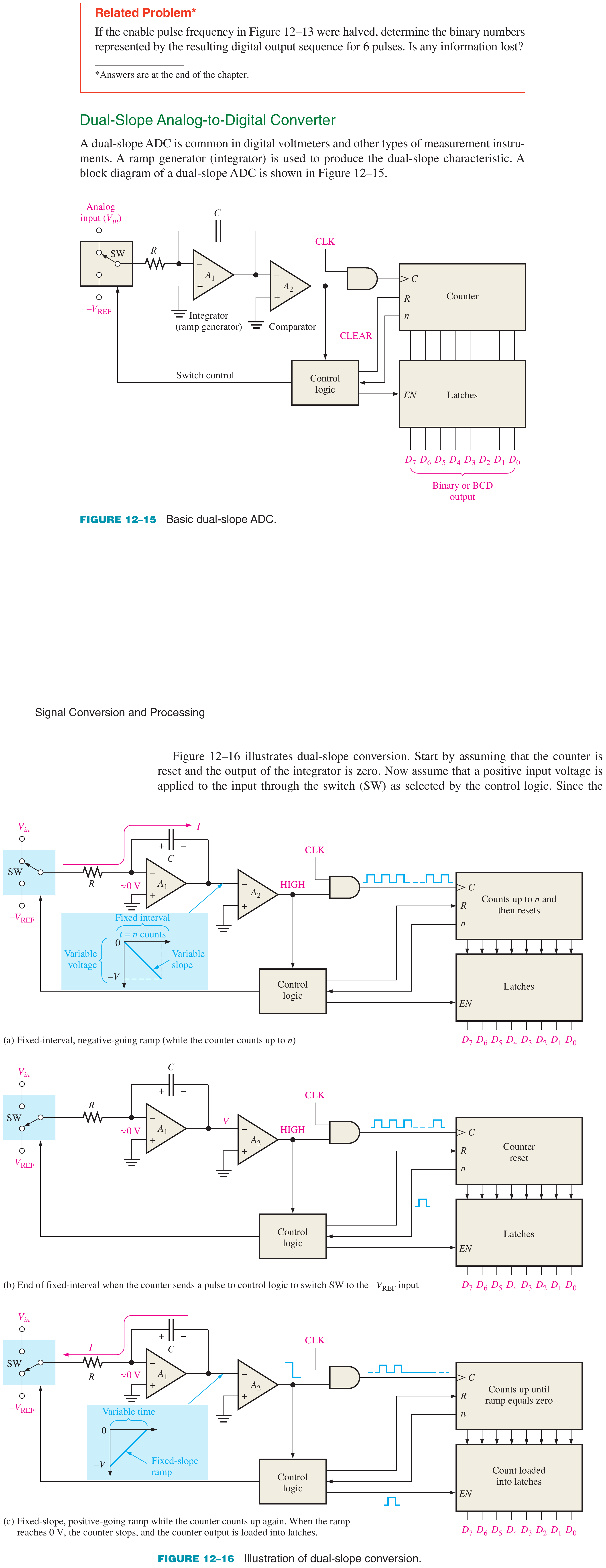
Operation (two phases):
Phase 1 — Integration (fixed time \(T_1 = 2^n\) clock cycles):
- Switch connects \(V_{in}\) to integrator input.
- Integrator output ramps up (or down) for exactly \(2^n\) clock cycles.
- Voltage at end of Phase 1: \(V_1 = -V_{in} \cdot T_1 / RC\)
Phase 2 — De-integration (variable time \(T_2\)):
- Switch connects \(-V_{ref}\) (opposite polarity) to integrator.
- Integrator output ramps back toward zero.
- Counter counts clock cycles until comparator detects zero crossing.
- Count value \(N = T_2\) is the digital output.
Key relationship:
Characteristics:
- Excellent noise rejection: Integrates input over a full cycle, rejecting 50/60 Hz noise.
- High accuracy: Errors in RC and clock frequency cancel out (ratio metric).
- Very slow: Conversion takes \(2 \times 2^n\) clock cycles in worst case.
- High resolution possible (up to 20+ bits).
Applications: Digital multimeters (DMMs), precision instrumentation, weighing scales.
Sigma-Delta (ΔΣ) ADC
Definition: A sigma-delta ADC uses oversampling (sampling at a rate much higher than Nyquist) combined with a noise-shaping modulator and a digital decimation filter to achieve very high resolution with simple analog components.
Key concepts:
- Oversampling ratio (OSR): Ratio of sampling frequency to Nyquist frequency. Typically 64× to 256×.
- 1-bit DAC: The modulator typically uses only a 1-bit quantizer (comparator), making the DAC perfectly linear.
- Noise shaping: The modulator pushes quantization noise to high frequencies (out of the band of interest).
- Digital filter: A low-pass digital decimation filter removes the shaped noise and downsamples to the output rate.
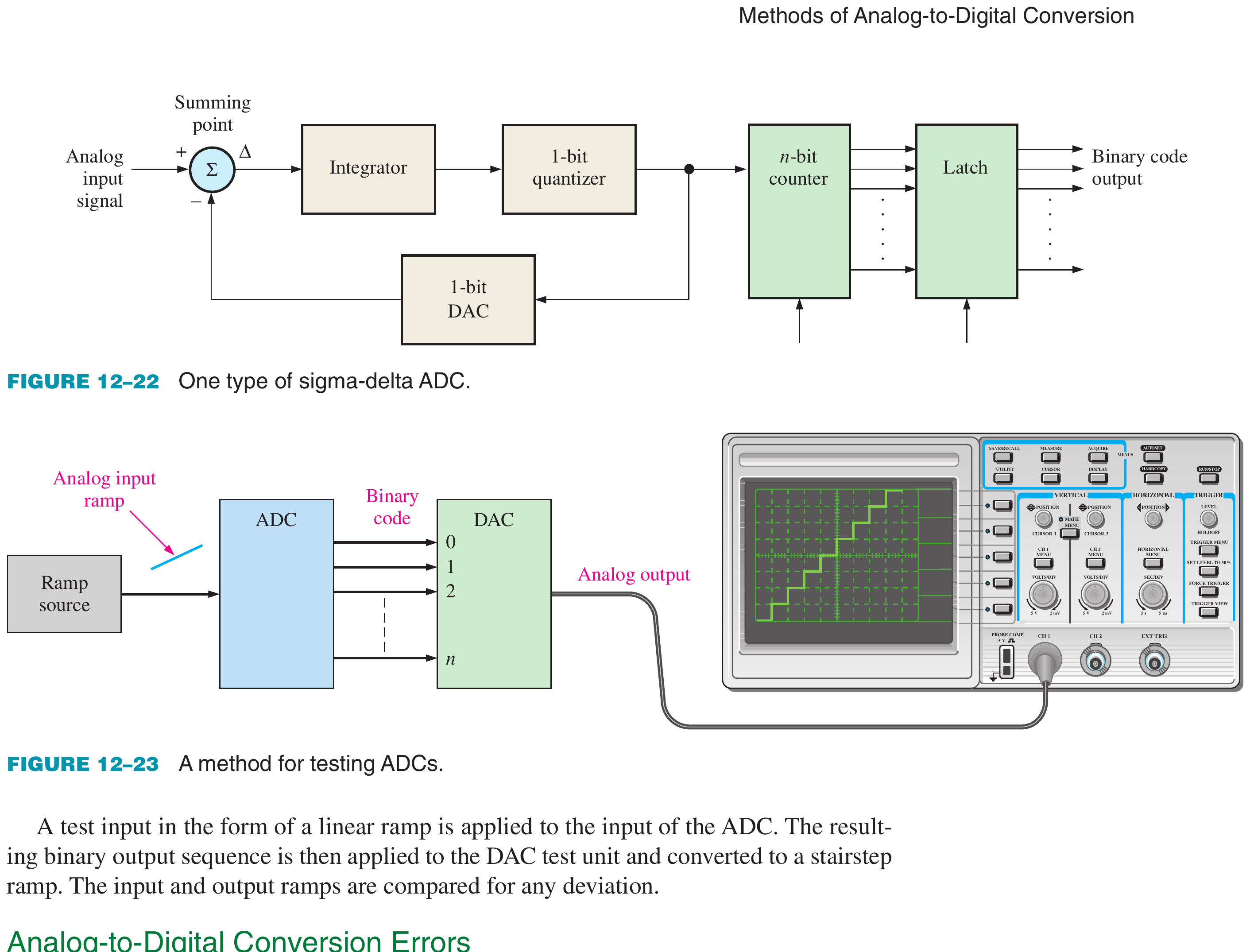
Characteristics:
- Very high resolution (16–24 bits).
- Excellent linearity (due to 1-bit DAC).
- Slow (due to oversampling and decimation).
- Simple analog circuit, complex digital processing.
Applications: Audio ADCs (CD/DVD), precision measurement, sensor interfaces, biomedical instruments.
ADC Types — Comparison
| Feature | Flash | SAR | Dual-Slope | Sigma-Delta |
|---|---|---|---|---|
| Speed | Fastest | Medium | Slowest | Slow |
| Resolution | Low (≤8 bits typical) | Medium-High (8–18 bits) | High (up to 20+ bits) | Very High (16–24 bits) |
| Conversion time | 1 clock cycle | \(n\) clock cycles | \(2^{n+1}\) cycles (worst) | Many cycles (oversampling) |
| Hardware complexity | Very high (\(2^n-1\) comparators) | Moderate | Low (analog) | Low analog, high digital |
| Cost | High | Moderate | Low | Low-Moderate |
| Noise rejection | Poor | Moderate | Excellent (integrating) | Excellent |
| Application | Video, radar | Data acquisition, embedded | DMM, precision instruments | Audio, sensors |
Key Exam Points — ADC
- Flash ADC: Fastest (1 cycle), needs \(2^n - 1\) comparators (exponential growth), limited to low resolution.
- SAR ADC: Binary search, \(n\) cycles, most popular general-purpose ADC.
- Dual-slope: Integrating type, very slow but excellent noise rejection, RC and clock errors cancel.
- Sigma-delta: Oversampling + noise shaping, highest resolution, used in audio and precision.
- Resolution = \(n\) bits → \(2^n\) quantization levels, step size \(\Delta = V_{ref}/2^n\).
Model Answer — Successive-Approximation A/D Conversion [10 marks, Eng. Sewa PYQ]
Exam-ready answer
Part A — A/D principle and key quantities [3 marks]
An analog-to-digital converter (ADC) samples an analog voltage, assigns it to one of a finite number of amplitude levels (quantisation), and encodes that level as a binary number. An ideal unipolar \(n\)-bit ADC spanning \(0\) to \(V_{ref}\) has
with ideal quantisation error bounded approximately by \(\pm\Delta/2\) when rounding to the nearest code. The sample-and-hold must keep \(V_{in}\) constant while a conversion is in progress.
Part B — SAR block diagram and operation [7 marks]
A successive-approximation register (SAR) ADC performs a binary search. It contains a sample-and-hold, comparator, SAR/control register, \(n\)-bit DAC, reference source, clock, start-of-conversion (SOC) and end-of-conversion (EOC) logic.
The held input is applied to one comparator input and the DAC estimate to the other. On SOC, the SAR tests bits from MSB to LSB:
- Clear the register, then tentatively set the MSB: code \(100\ldots0\), so \(V_{DAC}=V_{ref}/2\).
- If \(V_{in}\ge V_{DAC}\), retain that bit; if \(V_{in}<V_{DAC}\), clear it.
- Tentatively set the next lower bit while preserving all earlier decisions, compare again, and retain or clear it.
- Repeat through the LSB. After exactly \(n\) comparisons (approximately \(n\) clock periods, plus acquisition/control overhead), assert EOC and latch the final code.
For straight binary conversion,
Four-bit example: let \(V_{ref}=16\,\text{V}\) and \(V_{in}=10.4\,\text{V}\), so \(\Delta=1\,\text{V}\).
| Trial | \(V_{DAC}\) | Decision |
|---|---|---|
| 1000 | \(8\,\text{V}\) | \(10.4\ge8\): keep MSB |
| 1100 | \(12\,\text{V}\) | \(10.4<12\): clear \(b_2\) |
| 1010 | \(10\,\text{V}\) | \(10.4\ge10\): keep \(b_1\) |
| 1011 | \(11\,\text{V}\) | \(10.4<11\): clear LSB |
The result is \(1010_2=10_{10}\), representing \(10\,\text{V}\); the truncation error is \(0.4\,\text{V}\). Unlike a counter/ramp ADC, conversion time is fixed and independent of input magnitude.
Merits: moderate hardware, good 8–18-bit resolution, predictable latency, low power and a useful speed/accuracy compromise. Limitations: DAC settling, comparator offset, capacitor/resistor matching and S/H acquisition set accuracy; the input must not change appreciably during the search. SAR ADCs are widely used in microcontrollers, sensor interfaces, data acquisition and digital instrumentation.
Practice target: 16–18 minutes; spend about 5 minutes on the 3-mark principle and 11–13 minutes on the labeled block, bit sequence and example.
Model Answer — Flash, SAR and Dual-Slope ADC Comparison [10 marks]
Exam-ready answer
An ADC converts a sampled analog voltage into one of \(2^n\) digital codes. Flash, SAR and dual-slope converters differ mainly in whether they compare all thresholds simultaneously, search them successively, or measure an integration-time ratio.
Flash ADC: a resistor string generates \(2^n-1\) thresholds, the same number of comparators operate in parallel, and a priority encoder converts the thermometer code to binary.
It completes the analog decision in one parallel step and is the fastest architecture, but comparator count, input capacitance, area and power grow exponentially. Comparator offset and resistor matching limit practical high-resolution accuracy.
SAR ADC: one comparator, DAC and successive-approximation register perform an MSB-to-LSB binary search. Each tentative code is converted by the DAC and compared with the held input; one bit is decided per clock, so conversion needs approximately \(n\) clock periods and has fixed latency.
It offers moderate power and hardware with good 8–18-bit resolution, but accuracy depends on DAC settling/linearity, comparator offset and a stable held input.
Dual-slope ADC: an op-amp integrator first integrates unknown \(V_{in}\) for fixed time \(T_1\), then integrates an opposite-polarity reference until the output returns to zero. If \(T_2\) is the measured return time,
with polarity handled by the switching convention. RC and clock scale factors occur in both slopes and cancel in the ratio.
Integration averages interference, especially when \(T_1\) is an integer multiple of the \(50/60\,\text{Hz}\) mains period. The result is accurate and high resolution but very slow.
| Feature | Flash | SAR | Dual-slope |
|---|---|---|---|
| Principle | Parallel threshold comparison | Binary search with feedback DAC | Fixed-time integrate, timed de-integrate |
| Main analog hardware | \(2^n-1\) comparators plus ladder/encoder | One comparator, DAC, S/H and SAR | Integrator, comparator, switches, clock/counter |
| Conversion time | One comparator/encoder delay; essentially one step | About \(n\) clocks, fixed | Roughly \(T_1+T_2\), potentially thousands of clocks |
| Typical resolution | Low/medium, commonly up to about 8 bits | Medium/high, about 8–18 bits | High, often 16–20+ bits |
| Speed | Highest | Medium | Lowest |
| Power/area | Very high and exponential with \(n\) | Moderate | Low/moderate |
| Noise rejection | Poor; captures instantaneous noise | Moderate | Excellent due to averaging/integration |
| Main error limits | Comparator offsets and ladder mismatch | DAC linearity/settling and comparator offset | Reference, integrator leakage and auto-zero errors |
| Applications | Video, radar, oscilloscopes | General data acquisition, embedded sensors | Digital multimeters, weighing and precision DC measurement |
Numerical comparison: at \(n=12\), Flash would require \(2^{12}-1=4095\) comparators. With a \(1\,\text{MHz}\) decision clock, SAR needs about \(12\,\mu\text{s}\) plus acquisition. A dual-slope design using \(T_1=4096\) clocks needs \(4.096\,\text{ms}\) run-up and up to another \(4.096\,\text{ms}\) run-down, but gains strong noise rejection and ratio accuracy.
Conclusion: choose Flash when speed dominates, SAR for the best general-purpose speed/resolution/power compromise, and dual-slope when precision and interference rejection matter more than conversion rate.
Practice target: 16–18 minutes; sketch all three architectures, state each conversion law, and reproduce the comparison table.
Model Answer — Sigma-Delta Conversion, Oversampling and Noise Shaping [5 marks]
Exam-ready answer
A sigma-delta (\(\Delta\Sigma\)) ADC converts a narrow-band analog input into a high-rate, usually one-bit stream and then digitally filters it to obtain a high-resolution, low-rate word. It combines an analog feedback modulator with a digital low-pass/decimation filter.
For signal bandwidth \(B\) hertz and modulator sampling frequency \(f_s\), the oversampling ratio is
Conversion sequence:
- A summer subtracts the one-bit DAC feedback from \(V_{in}\).
- An integrator accumulates this error (the “sigma” operation).
- A one-bit quantiser/comparator emits 1 or 0; pulse density represents input amplitude. The one-bit DAC is inherently monotonic and feeds the corresponding reference level back.
- A digital low-pass filter removes out-of-band quantisation noise; the decimator then reduces sample rate and produces a multi-bit output.
Oversampling spreads approximately fixed quantisation-noise power over the much wider band \(0\) to \(f_s/2\). Only the small fraction inside \(0\) to \(B\) remains after digital filtering; oversampling alone improves in-band SNR by about \(3\,\text{dB}\) whenever OSR doubles.
Noise shaping improves this further. For a first-order loop, the linearised output is approximately
Since \(|1-e^{-j\omega}|\approx\omega\) near DC, the quantisation error \(E\) is suppressed in the signal band and pushed toward high frequencies, where the decimation filter removes it. A first-order modulator ideally gains about \(9\,\text{dB}\) in-band SNR per doubling of OSR (approximately 3 dB from oversampling plus 6 dB from shaping).
The result is excellent 16–24-bit resolution and linearity with simple analog circuitry. Limitations are restricted bandwidth, conversion latency, digital-filter complexity, clock-jitter sensitivity and possible idle tones/loop-stability issues. Applications include audio, precision sensors and biomedical measurement.
Practice target: 8–9 minutes; draw the feedback loop and clearly separate oversampling, shaping, filtering and decimation.