Thyristors and Controlled Rectifiers
Possible Exam Questions
Exam Questions and Answer Map
Questions marked [PYQ paper/year] were directly observed in past papers; [likely] means pattern-based prediction.
- Explain SCR construction, operation, V-I characteristics and triggering. [10] — [likely]
-
Model answer: SCR Construction and Characteristics
-
Explain SCR two-transistor regeneration and the turn-on condition. [5] — [likely]
-
Model answer: SCR Two-Transistor Regeneration
-
Explain full-wave and thyristor-controlled rectification, including average output and key performance measures. [10] — [PYQ 2079/2081]
- Model answers: Rectifier Characteristics · Full-Wave Bridge · Controlled Rectifier
1. Thyristor (SCR)
Likely Exam Question (10 marks)
"Explain the construction, operation, and V-I characteristics of a thyristor (SCR). How is it triggered?" OR "What is a thyristor? Draw its two-transistor analogy and explain the regenerative feedback mechanism."
SCR Definition
A thyristor (also called SCR — Silicon Controlled Rectifier) is a four-layer, three-junction (\(p\)-\(n\)-\(p\)-\(n\)), three-terminal (\(\text{Anode}\), \(\text{Cathode}\), \(\text{Gate}\)) semiconductor switching device. It acts as a bistable switch: once triggered into conduction, it remains ON (latches) until the current through it drops below a minimum value called the holding current (\(I_H\)).
Structure and Layers
The SCR has four alternating semiconductor layers:
- Junction \(J_1\): \(p_1\)-\(n_1\) (anode side)
- Junction \(J_2\): \(n_1\)-\(p_2\) (middle — this is the blocking junction)
- Junction \(J_3\): \(p_2\)-\(n_2\) (cathode side)
- Gate (G): Connected to the \(p_2\) layer.
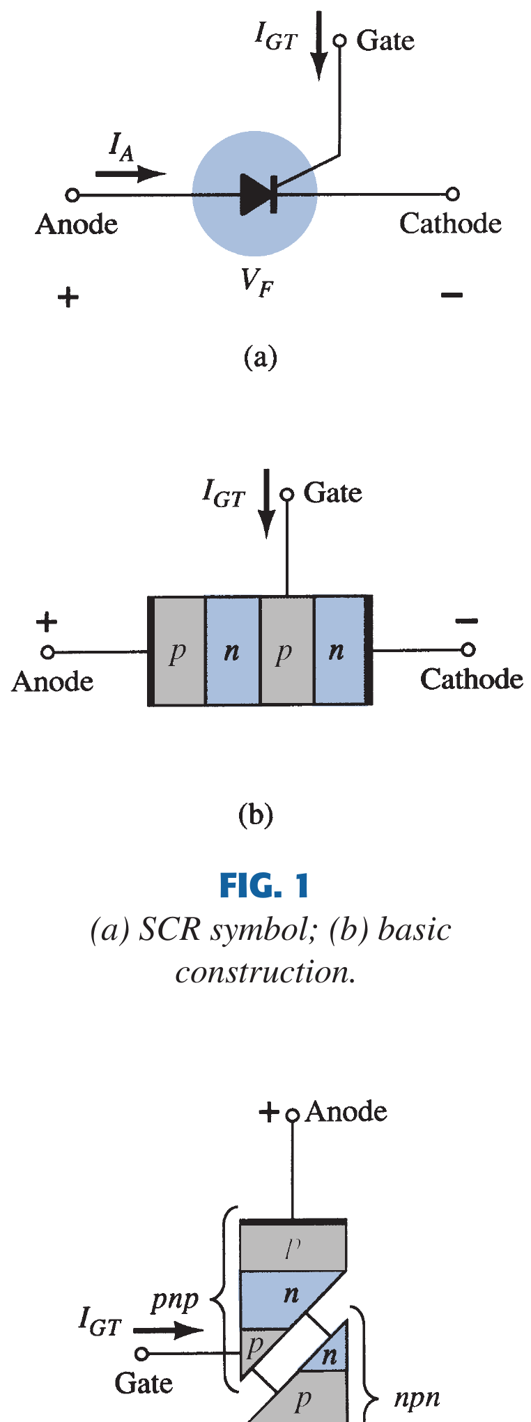
Two-Transistor Analogy
The SCR can be modelled as two interconnected transistors: a \(p\)-\(n\)-\(p\) transistor (\(T_1\)) and an \(n\)-\(p\)-\(n\) transistor (\(T_2\)):
- \(T_1\) (PNP): Emitter = Anode (\(p_1\)), Base = \(n_1\), Collector = \(p_2\)
- \(T_2\) (NPN): Emitter = Cathode (\(n_2\)), Base = \(p_2\) (Gate), Collector = \(n_1\)
The collector of each transistor is connected to the base of the other, forming a positive feedback (regenerative) loop:
Triggering mechanism: A small gate current \(I_G\) into the base of \(T_2\) causes \(T_2\) to conduct → its collector current flows into the base of \(T_1\) → \(T_1\) conducts → its collector current further increases the base current of \(T_2\) → regenerative feedback → both transistors saturate → SCR latches ON.
Condition for turn-ON (from two-transistor model):
where \(\alpha_1\) and \(\alpha_2\) are the current gains of \(T_1\) and \(T_2\). When this condition is met, the loop gain reaches 1 and regeneration occurs.
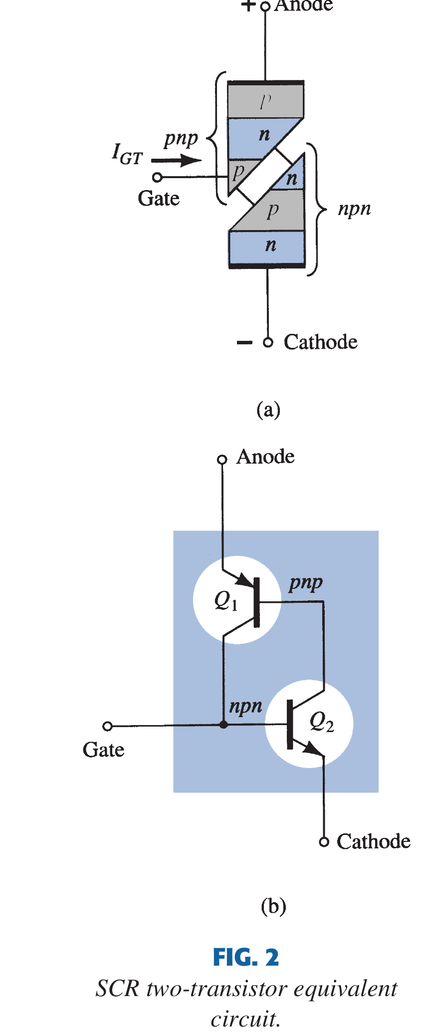

Book-grounded regeneration picture
Splitting the inner junctions gives a PNP transistor whose collector drives the NPN base and an NPN transistor whose collector drives the PNP base. Gate current starts the loop; increasing collector currents reinforce one another until the anode current is self-sustaining. The gate can trigger turn-on but cannot normally force a conducting SCR off.
Source figure: Boylestad/Nashelsky, Electronic Devices and Circuit Theory (11th ed.), PDF p. 875.
V-I Characteristics
The V-I characteristic of an SCR has three distinct regions:
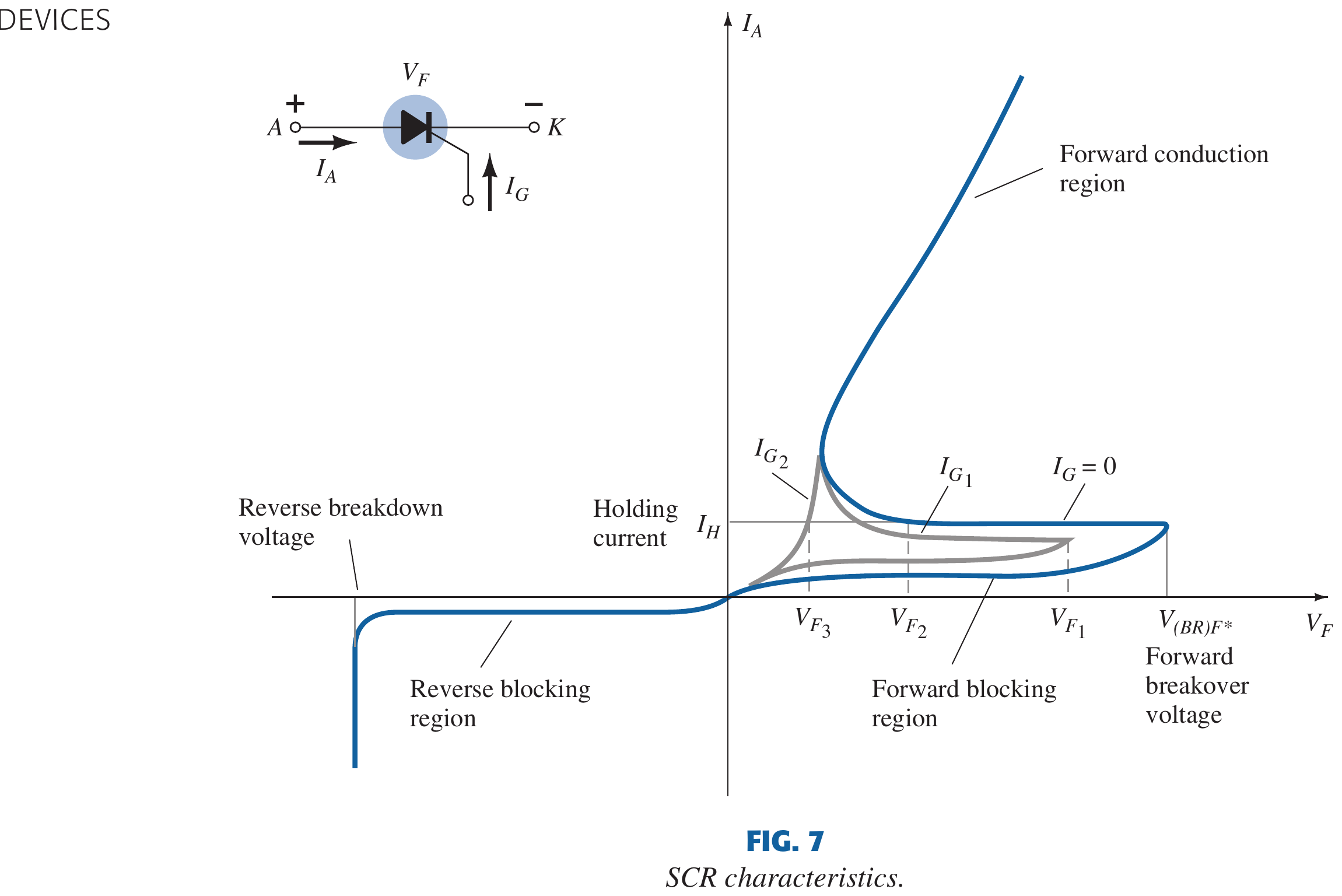
1. Forward Blocking (OFF State) — \(I_G = 0\):
- Anode positive w.r.t. cathode.
- \(J_1\) and \(J_3\) are forward-biased; \(J_2\) is reverse-biased (blocking junction).
- Only a small leakage current flows.
- The SCR blocks forward voltage up to the forward breakover voltage (\(V_{BO}\)).
2. Forward Conduction (ON State):
- When \(V_{AK} = V_{BO}\) (or when gate current \(I_G\) is applied): \(J_2\) breaks down → regeneration occurs → SCR turns ON.
- Voltage drops to a low value (~1–2 V, similar to a forward-biased diode).
- The SCR remains ON as long as the anode current \(I_A > I_H\) (holding current).
- Once ON, the gate has no further control — the SCR can only be turned OFF by reducing \(I_A < I_H\).
3. Reverse Blocking:
- Anode negative w.r.t. cathode.
- \(J_1\) and \(J_3\) are reverse-biased; \(J_2\) is forward-biased.
- Only leakage current flows until reverse breakdown voltage is reached (destructive).
SCR Turn-ON Methods
| Method | Description |
|---|---|
| Gate triggering | Apply a current pulse to the gate → most common and controlled method |
| Forward breakover | Increase \(V_{AK}\) beyond \(V_{BO}\) → \(J_2\) avalanche breakdown (undesirable, may damage) |
| \(dV/dt\) triggering | Rapid rate of voltage change charges \(J_2\) junction capacitance → displacement current triggers SCR |
| Temperature | Increased temperature raises leakage current → eventually triggers regeneration |
| Light triggering | Photons generate electron-hole pairs at \(J_2\) → used in Light-Activated SCR (LASCR) |
SCR Turn-OFF (Commutation)
The SCR can only be turned OFF by reducing anode current below the holding current. Two methods:
- Natural commutation: In AC circuits, the current naturally passes through zero every half cycle → SCR turns OFF.
- Forced commutation: In DC circuits, an external circuit (LC oscillator, auxiliary SCR) forces the anode current to zero.
Key SCR Parameters
| Parameter | Symbol | Description |
|---|---|---|
| Forward breakover voltage | \(V_{BO}\) | Max forward voltage before spontaneous turn-ON |
| Holding current | \(I_H\) | Min anode current to maintain ON state |
| Latching current | \(I_L\) | Min anode current to sustain ON state immediately after triggering (> \(I_H\)) |
| Gate trigger current | \(I_{GT}\) | Min gate current to turn ON the SCR |
| Gate trigger voltage | \(V_{GT}\) | Min gate voltage to turn ON the SCR |
Key Exam Points — SCR
- Four-layer \(p\)-\(n\)-\(p\)-\(n\) device; three junctions (\(J_1\), \(J_2\), \(J_3\)); three terminals (A, K, G).
- Two-transistor analogy: PNP + NPN with regenerative feedback; turns ON when \(\alpha_1 + \alpha_2 = 1\).
- Gate triggering is the most common turn-ON method.
- Once ON, gate loses control — OFF only when \(I_A < I_H\).
- AC circuits: natural commutation. DC circuits: forced commutation.
2. Full-Wave Bridge Rectifier
Likely Exam Question (5 marks)
"Explain the working principle of a full-wave bridge rectifier with the necessary circuit diagram." (NTC 2079 / Eng. Sewa 2082/83)
A full-wave bridge rectifier uses four diodes so that current through the load flows in the same direction during both half-cycles of the AC input. It does not require a center-tapped transformer.
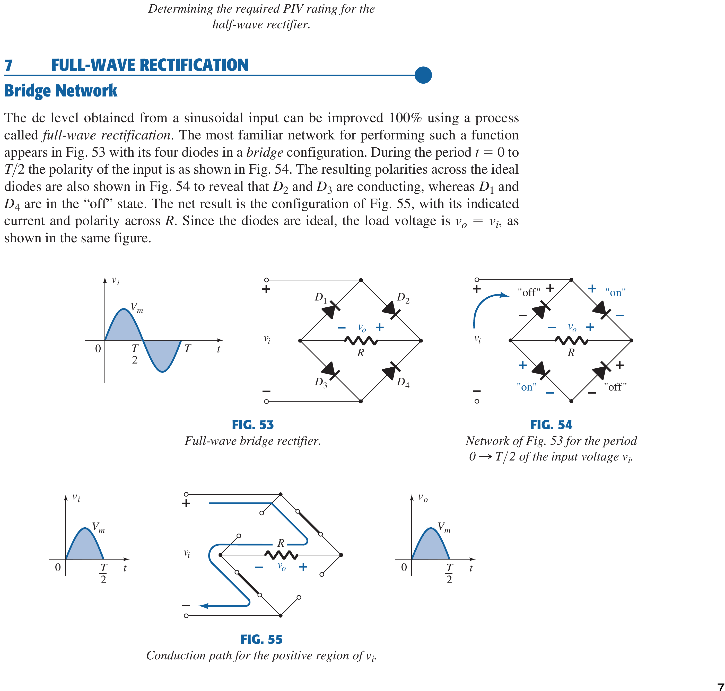
| Input half-cycle | Conducting diodes | Load-current path |
|---|---|---|
| Terminal A positive | \(D_1\) and \(D_3\) | A → \(D_1\) → \(R_L\) → \(D_3\) → B |
| Terminal B positive | \(D_2\) and \(D_4\) | B → \(D_2\) → \(R_L\) → \(D_4\) → A |
For ideal diodes:
Minimum Exam Labels
Mark the four diodes, AC terminals, load \(R_L\), output polarity, conducting pair in each half-cycle, and the full-wave output waveform.
3. Thyristor Controlled Rectifier Circuits
Likely Exam Question (10 marks)
"Explain the working of a single-phase half-wave controlled rectifier with an SCR. Derive the expression for average output voltage." OR "Compare half-wave and full-wave thyristor controlled rectifiers."
Controlled-Rectifier Definition
A thyristor controlled rectifier uses SCRs instead of diodes in rectifier circuits. By controlling the firing angle (\(\alpha\)) — the point in the AC cycle at which the gate pulse is applied — the average DC output voltage can be varied from maximum (same as an uncontrolled rectifier) to zero.
Single-Phase Half-Wave Controlled Rectifier (with R load)
Circuit: An SCR in series with the load (\(R\)) and AC supply \(V_m \sin\omega t\).
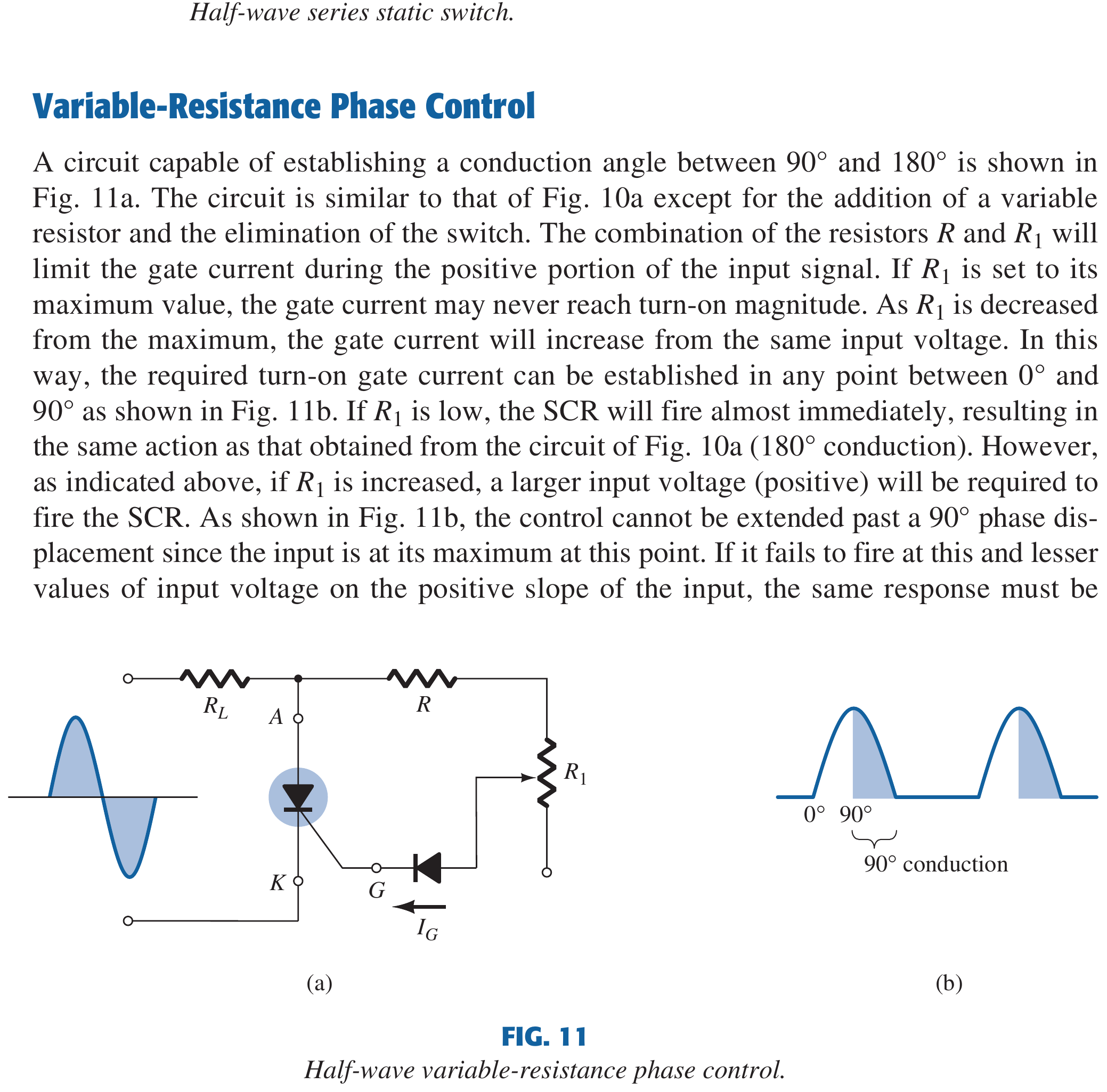
Operation:
- Positive half cycle (\(0\) to \(\pi\)): The anode is positive, but the SCR remains OFF until a gate trigger pulse is applied at angle \(\alpha\) (the firing angle).
- At \(\omega t = \alpha\): gate pulse applied → SCR turns ON → current flows through load.
- SCR conducts from \(\alpha\) to \(\pi\) (current follows the sine wave shape).
- At \(\omega t = \pi\): current tries to go negative → drops below \(I_H\) → SCR turns OFF (natural commutation).
- Negative half cycle (\(\pi\) to \(2\pi\)): SCR is reverse-biased → no conduction.
Average output voltage:
Derivation:
Special cases:
- \(\alpha = 0°\): \(V_{dc} = V_m/\pi\) (same as uncontrolled half-wave rectifier)
- \(\alpha = 90°\): \(V_{dc} = V_m/(2\pi)\) (half of maximum)
- \(\alpha = 180°\): \(V_{dc} = 0\) (no output)
Single-Phase Full-Wave Controlled Rectifier
Center-tap configuration: Two SCRs with a center-tapped transformer. Each SCR conducts for one half of the AC cycle (shifted by \(\alpha\)).
Bridge configuration: Four devices — two SCRs + two diodes (half-controlled bridge) or four SCRs (fully controlled bridge).
Average output voltage (full-wave, R load):
This is double the half-wave value because both halves of the AC cycle contribute.
Special cases:
- \(\alpha = 0°\): \(V_{dc} = 2V_m/\pi\) (same as uncontrolled full-wave rectifier)
- \(\alpha = 90°\): \(V_{dc} = V_m/\pi\)
Full-Controlled vs Half-Controlled Bridge
| Configuration | Devices | Control Range | Regeneration |
|---|---|---|---|
| Half-controlled | 2 SCRs + 2 diodes | \(\alpha = 0°\) to \(180°\), \(V_{dc} \geq 0\) | Not possible |
| Fully controlled | 4 SCRs | \(\alpha = 0°\) to \(180°\), \(V_{dc}\) can be negative (with RL load) | Possible (power returned to source) |
Three-Phase Controlled Rectifier (Brief Overview)
For high-power industrial applications, three-phase rectifiers are used:
Three-phase half-wave (3-pulse): 3 SCRs, one per phase.
Three-phase full-wave bridge (6-pulse): 6 SCRs.
Comparison — Half-Wave vs Full-Wave Controlled Rectifier
| Feature | Half-Wave | Full-Wave |
|---|---|---|
| No. of SCRs | 1 | 2 (center-tap) or 4 (bridge) |
| Conduction per cycle | \((\pi - \alpha)\) radians | \(2(\pi - \alpha)\) radians |
| Avg. output voltage | \(V_m(1+\cos\alpha)/(2\pi)\) | \(V_m(1+\cos\alpha)/\pi\) |
| Ripple frequency | \(f\) | \(2f\) |
| Ripple magnitude | Higher | Lower (easier to filter) |
| Efficiency | Lower | Higher |
| Transformer utilisation | Poor | Better |
Key Exam Points — Controlled Rectifiers
- Firing angle \(\alpha\) controls the average output voltage.
- Half-wave: \(V_{dc} = V_m(1+\cos\alpha)/(2\pi)\). Full-wave: \(V_{dc} = V_m(1+\cos\alpha)/\pi\).
- At \(\alpha = 0°\): output equals uncontrolled rectifier. At \(\alpha = 180°\): output = 0.
- SCR turns OFF naturally at current zero (AC circuits) — natural commutation.
- Full-wave has lower ripple, higher efficiency, better transformer utilisation.
7. Rectifier Characteristics
Likely Exam Question (5 marks)
"Explain the basic characteristics of a rectifier with mathematical expressions (ripple factor, efficiency, PIV)."
Key Rectifier Parameters
| Parameter | Definition | Formula |
|---|---|---|
| DC output voltage (\(V_{dc}\)) | Average value of the rectified waveform | Half-wave: \(V_m/\pi\); Full-wave: \(2V_m/\pi\) |
| RMS output voltage (\(V_{rms}\)) | Root-mean-square of the rectified waveform | Half-wave: \(V_m/2\); Full-wave: \(V_m/\sqrt{2}\) |
| Ripple factor (\(\gamma\)) | Measure of AC content remaining in the DC output | \(\gamma = \sqrt{\left(\dfrac{V_{rms}}{V_{dc}}\right)^2 - 1}\) |
| Rectifier efficiency (\(\eta\)) | Ratio of DC power delivered to load vs total AC input power | \(\eta = \dfrac{P_{dc}}{P_{ac}} = \dfrac{V_{dc}^2/R_L}{V_{rms}^2/R_L}\) |
| Peak Inverse Voltage (PIV) | Maximum reverse voltage across a non-conducting diode | Depends on topology |
| Transformer Utilisation Factor (TUF) | DC power output / VA rating of the transformer | Indicates how well transformer is utilised |
Half-Wave vs Full-Wave Comparison
| Parameter | Half-Wave | Full-Wave (Bridge) |
|---|---|---|
| \(V_{dc}\) | \(V_m/\pi = 0.318\,V_m\) | \(2V_m/\pi = 0.636\,V_m\) |
| \(\gamma\) | 1.21 (121%) | 0.48 (48%) |
| \(\eta\) (max) | 40.6% | 81.2% |
| PIV per diode | \(V_m\) (centre-tap: \(2V_m\)) | \(V_m\) |
| Ripple frequency | \(f\) | \(2f\) |
| Diodes required | 1 | 4 (bridge) or 2 (centre-tap) |
Model Answer — SCR Construction, Operation, Characteristics and Triggering [10 marks]
Exam-ready answer
An SCR (silicon-controlled rectifier) is a unidirectional, latching power switch with four alternating semiconductor layers \(p_1n_1p_2n_2\), three junctions and terminals anode A, cathode K and gate G. A is connected to \(p_1\), K to \(n_2\), and G to the inner \(p_2\) layer near the cathode.
Operating States
- Reverse blocking: with A negative relative to K, \(J_1\) and \(J_3\) are reverse biased. Only reverse leakage flows until reverse breakdown, which is normally destructive.
- Forward blocking: with A positive and \(I_G=0\), \(J_1,J_3\) are forward biased but central \(J_2\) is reverse biased. The SCR blocks up to forward breakover \(V_{BO}\), apart from leakage.
- Forward conduction: a positive gate pulse injects carriers into \(p_2\). The equivalent PNP/NPN pair regenerates: each transistor's collector drives the other's base. \(J_2\) loses its blocking action and the device snaps to a low on-state voltage, typically about \(1\)–\(2\,\text{V}\).
Increasing gate current reduces the forward voltage needed for turn-on. Immediately after triggering, anode current must rise above the latching current \(I_L\) before the gate pulse is removed. Once latched, the gate cannot turn the SCR off; conduction continues while \(I_A>I_H\), where holding current \(I_H<I_L\). Turn-off requires current below \(I_H\) for the specified turn-off time: naturally at AC current zero or by forced commutation in DC circuits.
Triggering methods:
- Gate triggering: a rated positive \(G\)-to-\(K\) current pulse; this is the normal controllable method.
- Forward breakover: raise \(V_{AK}\) to \(V_{BO}\); avoided in normal service because avalanche stresses the device.
- \(dv/dt\) triggering: junction capacitance current \(i=C_jdv/dt\) can start regeneration; an RC snubber limits it.
- Light (LASCR), temperature or radiation may also generate carriers, but unintended thermal triggering is a hazard.
Important ratings/protection: repetitive peak forward- and reverse-blocking voltages \(V_{DRM},V_{RRM}\); average/RMS/surge on-state current; gate trigger current/voltage \(I_{GT},V_{GT}\); \(I_L,I_H\); maximum \(dv/dt\), \(di/dt\) and junction temperature. A series inductance limits turn-on \(di/dt\) because conduction initially occupies a small junction area; a snubber limits false \(dv/dt\) turn-on; heat sinking keeps \(T_j\) within rating.
Check: if a gate pulse produces \(I_A=30\,\text{mA}\) while \(I_L=25\,\text{mA}\), the device remains on after the pulse. If load current later falls below, for example, \(I_H=10\,\text{mA}\) for sufficient time, it turns off. This distinguishes latching from holding current.
SCRs control rectifiers, heaters, lamp dimmers and motor drives. They handle high power with low on loss, but conduct only one direction and lack gate turn-off capability.
Practice target: 18 minutes; draw the structure and V-I curve, explain all three regions, regeneration, triggering, latching/holding and four key ratings.
Model Answer — SCR Two-Transistor Regeneration [5 marks]
Exam-ready answer
The SCR's \(p_1n_1p_2n_2\) layers can be separated into a PNP transistor \(T_1\) and an NPN transistor \(T_2\). The collector of each drives the base of the other, forming a positive-feedback loop; the gate injects current into the base region of \(T_2\).
Let common-base gains be \(\alpha_1,\alpha_2\) and collector leakage currents be \(I_{CBO1},I_{CBO2}\). Then
Since the anode current supplies the two cross-coupled collector/base paths, \(I_A=I_{C1}+I_{C2}\). Hence
Initially \(\alpha_1+\alpha_2<1\), so only leakage flows. A gate pulse increases \(T_2\) current; its collector drives \(T_1\), whose collector then supplies still more \(T_2\) base current. As current rises, both gains rise and
making the denominator very small. The ideal equation suggests unbounded current, but the external load and transistor saturation limit it: physically both transistors switch hard on. After regeneration, internal collector currents replace the gate drive, so the SCR latches. It remains on after \(I_G\) is removed provided \(I_A>I_L\) initially and later \(I_A>I_H\); otherwise regeneration collapses and it returns to blocking.
Practice target: 8 minutes; draw the cross-coupling, derive the current equation and explain why the mathematical singularity means saturation/latching, not infinite current.
Model Answer — Rectifier Performance Characteristics [5 marks, Eng. Sewa PYQ]
Exam-ready answer
A rectifier converts AC to unidirectional voltage. For periodic output \(v_o(\theta)\),
The RMS AC ripple component is \(V_{ac}=\sqrt{V_{rms}^2-V_{dc}^2}\), hence
Ideal rectification efficiency is
and PIV is the greatest reverse voltage that a nonconducting diode must withstand.
| Ideal quantity | Half-wave | Full-wave bridge |
|---|---|---|
| \(V_{dc}\) | \(V_m/\pi=0.318V_m\) | \(2V_m/\pi=0.637V_m\) |
| \(V_{rms}\) | \(V_m/2\) | \(V_m/\sqrt2\) |
| Ripple factor \(\gamma\) | \(\sqrt{\pi^2/4-1}=1.21\) | \(\sqrt{\pi^2/8-1}=0.482\) |
| Maximum \(\eta\) | \(4/\pi^2=40.6\%\) | \(8/\pi^2=81.2\%\) |
| Ripple frequency | \(f\) | \(2f\) |
| PIV per diode | \(V_m\) | \(V_m\) |
For a centre-tapped full-wave rectifier, PIV is \(2V_m\) per diode when \(V_m\) is the peak of one half-secondary. Real diode drops and winding resistance reduce \(V_{dc}\) and efficiency; a filter lowers load ripple but changes diode-current pulses and transformer utilisation.
Practice target: 8 minutes; derive both ripple factors from the RMS/DC values and keep bridge PIV distinct from centre-tapped PIV.
Model Answer — Full-Wave Bridge Rectifier Operation [5 marks, PYQ 2079 / Eng. Sewa]
Exam-ready answer
A full-wave bridge rectifier uses four diodes to reverse the negative input half-cycle at the load, so load current always has the same polarity. It needs no centre-tapped transformer.
| Input condition | Conducting pair | Load-current path |
|---|---|---|
| AC terminal A positive to B | \(D_1,D_3\) | A \(\to D_1\to R_L\to D_3\to\) B |
| AC terminal B positive to A | \(D_2,D_4\) | B \(\to D_2\to R_L\to D_4\to\) A |
For ideal diodes, \(v_o=V_m|\sin\theta|\). Therefore
Two diodes conduct in series, so a practical silicon bridge has approximately \(v_o\approx |v_s|-2V_D\) whenever \(|v_s|>2V_D\). Compared with a centre-tapped full-wave circuit, the bridge uses the whole secondary on both half-cycles, has better transformer utilisation and only \(V_m\) diode PIV, but incurs two forward drops instead of one. A capacitor or LC filter may smooth the pulsating DC, followed by regulation.
Check: for \(V_m=20\,\text{V}\), ideal \(V_{dc}=40/\pi=12.73\,\text{V}\) and every diode should be rated safely above \(20\,\text{V}\) reverse voltage, with margin for surges.
Practice target: 8 minutes; draw and label both conduction paths, then derive average voltage, ripple frequency and diode PIV.
Model Answer — Thyristor-Controlled Rectifier and Average Output [10 marks, PYQ 2081]
Exam-ready answer
A controlled rectifier replaces rectifier diodes with SCRs so a gate delay controls the fraction of each AC cycle delivered to the load. Let \(v_s=V_m\sin\theta\), where \(\theta=\omega t\), and let firing angle \(\alpha\) be measured from the natural zero crossing.
For a half-wave circuit with a purely resistive load, the forward-biased SCR remains off from \(0\) to \(\alpha\). A gate pulse at \(\alpha\) turns it on; current \(i_o=v_s/R\) then flows from \(\alpha\) to \(\pi\). At \(\pi\), current naturally reaches zero and falls below \(I_H\), so the SCR commutates off. It is reverse biased throughout the negative half-cycle.
Thus
and the cycle average is
It reduces from \(V_m/\pi\) at \(\alpha=0\) to zero at \(\alpha=\pi\).
In a single-phase full-wave bridge with an R load, diagonal SCR pairs are fired at \(\alpha\) and \(\pi+\alpha\). The two positive load-voltage segments each last from firing to the following supply zero:
twice the half-wave value, with ripple frequency \(2f\).
A different formula applies to a fully controlled bridge with a sufficiently inductive load and continuous current. Each pair conducts for \(\pi\) radians and output may become negative during part of the cycle, giving
This distinction is essential: \(V_m(1+\cos\alpha)/\pi\) is the discontinuous R-load result, while \(2V_m\cos\alpha/\pi\) is the continuous-current full-converter result.
Numerical check: for \(V_m=325\,\text{V}\) and \(\alpha=60^\circ\), half-wave R-load average is \(325(1+0.5)/(2\pi)=77.6\,\text{V}\); full-wave R-load average is \(155.2\,\text{V}\). Under continuous current, the full converter gives \(2(325)(0.5)/\pi=103.5\,\text{V}\).
Increasing \(\alpha\) lowers output and worsens input power factor/harmonics. Full-wave operation gives greater average output and lower ripple than half-wave. Applications include controlled DC drives, battery chargers, heaters and HVDC converters; gate isolation, snubbers, fuses and heat sinks are required in practice.
Practice target: 18 minutes; draw both circuits/waveforms, derive the half-wave integral and state the two full-wave load-dependent formulas without mixing them.