Registers, Counters and Sequence Generators
Possible Exam Questions
Exam Questions and Answer Map
Questions marked [PYQ paper/year] were directly observed in past papers; [likely] means pattern-based prediction, not a claimed past question. Rehearse each answer plan closed-book, then check the full answer via the links.
-
What is a shift register? Explain the four types (SISO, SIPO, PISO, PIPO) with applications. [5] — [likely]
-
Answer plan: Define shift register (cascade of FFs, data shifts one stage per clock) → SISO: serial in/out, time delay → SIPO: serial-to-parallel conversion → PISO: parallel-to-serial conversion → PIPO: buffer/temporary storage → draw basic 4-bit SISO diagram → tabulate applications.
-
Model answer: Shift-Register Types and Applications
-
Draw the circuit of a 2-bit (asynchronous) counter and explain it. [5] — [PYQ 2082]
-
Answer plan: Draw 2 T/JK flip-flops → FF0 clocked by external clock → FF1 clocked by \(\overline{Q_0}\) (falling edge of FF0) → draw timing diagram showing 4-state sequence (00→01→10→11→00) → explain ripple delay propagation → state mod-4 count.
-
Model answer: Two-Bit Asynchronous Ripple Counter
-
Differentiate synchronous and asynchronous (ripple) counters. [5] — [likely]
-
Answer plan: Ripple: each FF clocked by previous FF output → cumulative delay → simple but slow. Synchronous: all FFs share common clock → change simultaneously → faster, glitch-free → needs combinational logic for inputs → tabulate speed, complexity, applications.
-
Model answer: Synchronous and Ripple Counter Comparison
-
Design a synchronous mod-5 counter using JK flip-flops (state table, K-maps, circuit). [10] — [likely]
-
Answer plan: 3 FFs (\(Q_2 Q_1 Q_0\)), states 000–100 → write state transition table → use JK excitation table to find required J, K for each FF at each transition → draw K-maps for \(J_2, K_2, J_1, K_1, J_0, K_0\) → minimise → draw circuit → verify with timing diagram.
-
Model answer: Synchronous Mod-5 JK Counter Design
-
What is a sequence generator? Explain the ring counter and Johnson counter. [5] — [likely]
-
Answer plan: Define sequence generator (circuit producing predefined output sequence) → Ring counter: circular shift register, one-hot pattern, \(n\) FFs → \(n\) states → Johnson (twisted ring): complement of last FF fed back, \(n\) FFs → \(2n\) states → compare states, decoding complexity, self-correction.
- Model answer: Ring and Johnson Sequence Generators
1. Shift Registers
Likely Exam Question (5 marks)
"What is a shift register? Explain the four types (SISO, SIPO, PISO, PIPO) with applications."
Shift-Register Definition
A shift register is a group of flip-flops (usually D flip-flops) connected in cascade (output of one connected to input of the next), where data is shifted from one flip-flop to the next with each clock pulse. An \(n\)-bit shift register uses \(n\) flip-flops and can store \(n\) bits of data.
Types of Shift Registers
| Type | Full Name | Input Method | Output Method | Application |
|---|---|---|---|---|
| SISO | Serial-In, Serial-Out | One bit per clock | One bit per clock (from last FF) | Time delay, serial data transfer |
| SIPO | Serial-In, Parallel-Out | One bit per clock | All bits simultaneously | Serial-to-parallel conversion |
| PISO | Parallel-In, Serial-Out | All bits loaded at once | One bit per clock | Parallel-to-serial conversion |
| PIPO | Parallel-In, Parallel-Out | All bits loaded at once | All bits simultaneously | Temporary storage, data buffering |
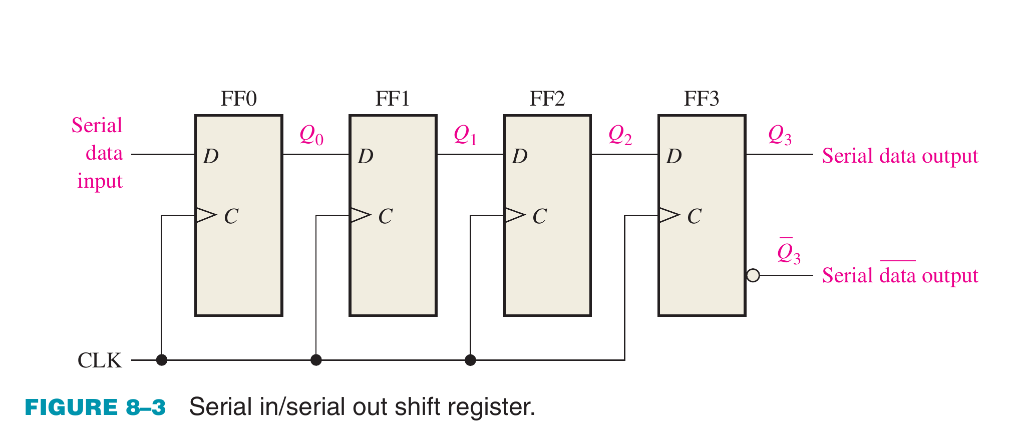

Book-grounded data-motion rule
On each active clock edge, every stage copies the previous stage value simultaneously; values do not race through all four stages in one edge. The first input bit reaches the serial output after four active edges in a four-stage SISO register.
Source figure: Floyd, Digital Fundamentals (11th ed.), PDF p. 452.
SISO — Serial-In Serial-Out
Data enters the first flip-flop serially (one bit per clock). With each clock pulse, data shifts one position to the right. After \(n\) clock pulses, the first bit appears at the output. Acts as a time delay of \(n\) clock periods.
SIPO — Serial-In Parallel-Out
Data enters serially. After \(n\) clock pulses, all \(n\) bits are stored in the register and are available simultaneously at the parallel outputs. Used for serial-to-parallel conversion (e.g., receiving serial data from a communication line and presenting it as a parallel byte).
PISO — Parallel-In Serial-Out
All \(n\) data bits are loaded into the register simultaneously (using a parallel load control). Then, with each clock pulse, data shifts out serially from the last flip-flop. Used for parallel-to-serial conversion (e.g., converting a parallel data bus to serial for transmission).
PIPO — Parallel-In Parallel-Out
Data is loaded in parallel and read out in parallel. Essentially a temporary storage register (buffer). Used for data buffering between systems operating at different speeds.
Bidirectional Shift Register
A bidirectional shift register can shift data either left or right based on a direction control signal. Achieved by adding multiplexers before each flip-flop input to select between the output of the left or right neighbour.
Common IC: 74194 — 4-bit universal shift register with four operating modes: parallel load, shift right, shift left, and hold (inhibit).
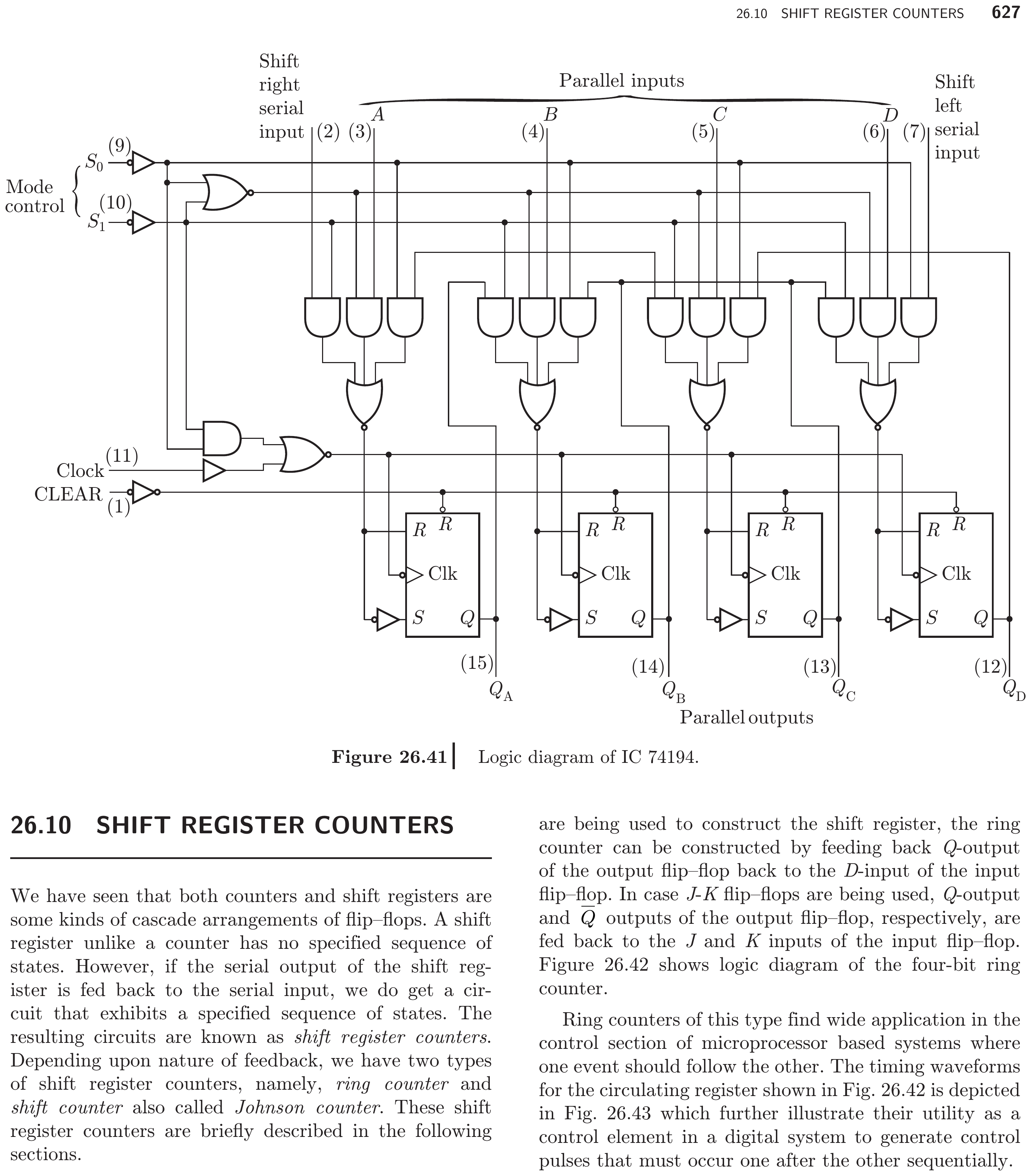
Special Shift Register Configurations
| Configuration | Description | Sequence Length |
|---|---|---|
| Ring counter | Output of last FF connected back to input of first FF. One '1' circulates. | \(n\) states for \(n\) FFs |
| Johnson (twisted ring) counter | Complemented output of last FF connected to input of first FF. | \(2n\) states for \(n\) FFs |
| LFSR (Linear Feedback Shift Register) | XOR of selected FF outputs fed back to input. | Up to \(2^n - 1\) states (pseudo-random sequence) |
Key Exam Points — Shift Registers
- \(n\) FFs = \(n\)-bit storage, data shifts one position per clock.
- SISO: serial in, serial out (delay line). SIPO: serial to parallel. PISO: parallel to serial. PIPO: buffer.
- Universal shift register (74194): all four modes + parallel load.
- Ring counter: \(n\) states; Johnson counter: \(2n\) states; LFSR: up to \(2^n-1\) states.
2. Counters
Likely Exam Question (10 marks)
"Design a synchronous mod-5 counter using JK flip-flops. Show the state table, K-maps, and circuit." OR "Compare ripple (asynchronous) and synchronous counters."
Counter Definition
A counter is a sequential circuit that goes through a prescribed sequence of states with each clock pulse, typically counting in binary. The number of distinct states in the sequence is called the modulus (mod) of the counter. A mod-\(N\) counter counts from 0 to \(N-1\) and then resets.
Asynchronous (Ripple) Counter
Definition: In an asynchronous (ripple) counter, only the first flip-flop is driven by the external clock. Each subsequent flip-flop is clocked by the output of the previous flip-flop. The clock signal "ripples" through the chain.
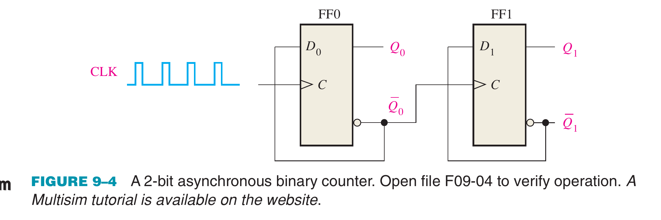

Book-grounded clock convention
State the triggering convention before deriving the sequence. In this positive-edge D-flip-flop realization, \(\overline{Q_0}\) clocks FF1; an equivalent falling-edge implementation can clock FF1 from \(Q_0\). Mixing those conventions reverses or corrupts the claimed count sequence.
Source figure: Floyd, Digital Fundamentals (11th ed.), PDF p. 501.
3-Bit Ripple Up-Counter — State Sequence:
| Clock Pulse | \(Q_2\) | \(Q_1\) | \(Q_0\) | Decimal |
|---|---|---|---|---|
| 0 | 0 | 0 | 0 | 0 |
| 1 | 0 | 0 | 1 | 1 |
| 2 | 0 | 1 | 0 | 2 |
| 3 | 0 | 1 | 1 | 3 |
| 4 | 1 | 0 | 0 | 4 |
| 5 | 1 | 0 | 1 | 5 |
| 6 | 1 | 1 | 0 | 6 |
| 7 | 1 | 1 | 1 | 7 |
| 8 | 0 | 0 | 0 | 0 (repeats) |
Modulus: \(2^n\) where \(n\) = number of flip-flops. 3 FFs → mod-8 (counts 0–7).
How it works: Each T flip-flop (with \(T=1\)) toggles on the falling edge of its clock. \(Q_0\) toggles on every external clock edge. \(Q_1\) toggles on every falling edge of \(Q_0\). \(Q_2\) toggles on every falling edge of \(Q_1\).
Limitations of Ripple Counter:
- Cumulative propagation delay: Total delay = \(n \times t_{pd}\). Outputs do not change simultaneously.
- Glitches (momentary incorrect outputs) occur during transitions.
- Maximum clock frequency: \(f_{\max} = 1/(n \times t_{pd})\).
- Not suitable for high-speed applications.
Synchronous Counter
Definition: In a synchronous counter, all flip-flops are driven by the same clock signal simultaneously. The count sequence is determined by the combinational logic connected to the flip-flop inputs. All outputs change at the same time (within one propagation delay of the clock edge).
Advantages over ripple counter:
- No cumulative delay — all FFs clock together.
- No glitches.
- Higher maximum operating frequency.
- Can implement any arbitrary count sequence.
Design Procedure for Synchronous Counters
Step 1: Determine the required state sequence and number of flip-flops needed (\(n\) FFs for up to \(2^n\) states).
Step 2: Draw the state table — list present state, next state, and required flip-flop inputs (using excitation tables).
Step 3: Use K-maps (Karnaugh maps) to simplify the Boolean expressions for each flip-flop input.
Step 4: Draw the circuit.
Mod-N Counter Using Reset
A simpler (but less elegant) approach: use a mod-\(2^n\) ripple counter and add a NAND gate that detects state \(N\) and immediately resets all flip-flops to 0.
Example — Mod-10 (Decade) Counter:
- Use a 4-bit ripple counter (mod-16).
- Detect state \(1010\) (decimal 10) using a NAND gate on \(Q_3\) and \(Q_1\).
- Feed NAND output to the CLR (clear) inputs of all flip-flops.
- Counter counts 0–9 then resets to 0 on reaching 10.
Common IC: 7490 (decade counter), 7493 (4-bit binary counter).
Up/Down Counter
An up/down counter can count in either direction (incrementing or decrementing) based on an UP/DOWN control input. The control signal selects which flip-flop output (normal or complemented) is used to clock the next stage.
Ripple vs Synchronous — Comparison
| Feature | Ripple (Asynchronous) | Synchronous |
|---|---|---|
| Clock | Only first FF clocked externally | All FFs clocked simultaneously |
| Speed | Slow (cumulative delay) | Fast (single propagation delay) |
| Glitches | Yes (during transitions) | No |
| Design complexity | Simple | More complex (needs combinational logic) |
| Max frequency | \(1/(n \times t_{pd})\) | \(1/t_{pd}\) |
| Arbitrary sequences | Difficult | Easy to implement |
Key Exam Points — Counters
- Ripple counter: clock ripples through FFs → cumulative delay, glitches, slow.
- Synchronous counter: all FFs share one clock → faster, no glitches, any sequence possible.
- Mod-\(N\) counter: \(\lceil\log_2 N\rceil\) flip-flops needed.
- Design steps: state table → excitation table → K-maps → circuit.
- JK excitation table is the most important for exam counter design problems.
3. Sequence Generators
Likely Exam Question (5 marks)
"What is a sequence generator? Explain ring counter and Johnson counter."
Sequence-Generator Definition
A sequence generator is a sequential circuit that produces a prescribed, repeating sequence of binary patterns at its outputs. It is typically built from shift registers with feedback.
Ring Counter
Definition: A ring counter is a shift register where the output of the last flip-flop is connected back to the input of the first flip-flop (circular shift), and only one flip-flop is set to 1 at any time (all others are 0). The single '1' circulates through the register.
For \(n\) flip-flops: \(n\) distinct states, each with exactly one '1'.
Example (4-bit ring counter):
| Clock | \(Q_3\) | \(Q_2\) | \(Q_1\) | \(Q_0\) |
|---|---|---|---|---|
| 0 | 1 | 0 | 0 | 0 |
| 1 | 0 | 1 | 0 | 0 |
| 2 | 0 | 0 | 1 | 0 |
| 3 | 0 | 0 | 0 | 1 |
| 4 | 1 | 0 | 0 | 0 (repeats) |
Disadvantage: Uses \(n\) flip-flops for only \(n\) states (wasteful — a binary counter uses \(n\) FFs for \(2^n\) states).
Advantage: No decoding logic needed — each output directly represents one state. Self-decoding.
Johnson (Twisted Ring) Counter
Definition: A Johnson counter (or twisted ring counter or Möbius counter) is a shift register where the complemented output of the last flip-flop is fed back to the input of the first flip-flop.
For \(n\) flip-flops: \(2n\) distinct states.
Example (4-bit Johnson counter):
| Clock | \(Q_3\) | \(Q_2\) | \(Q_1\) | \(Q_0\) |
|---|---|---|---|---|
| 0 | 0 | 0 | 0 | 0 |
| 1 | 1 | 0 | 0 | 0 |
| 2 | 1 | 1 | 0 | 0 |
| 3 | 1 | 1 | 1 | 0 |
| 4 | 1 | 1 | 1 | 1 |
| 5 | 0 | 1 | 1 | 1 |
| 6 | 0 | 0 | 1 | 1 |
| 7 | 0 | 0 | 0 | 1 |
| 8 | 0 | 0 | 0 | 0 (repeats) |
4 FFs → 8 states (double that of a ring counter).
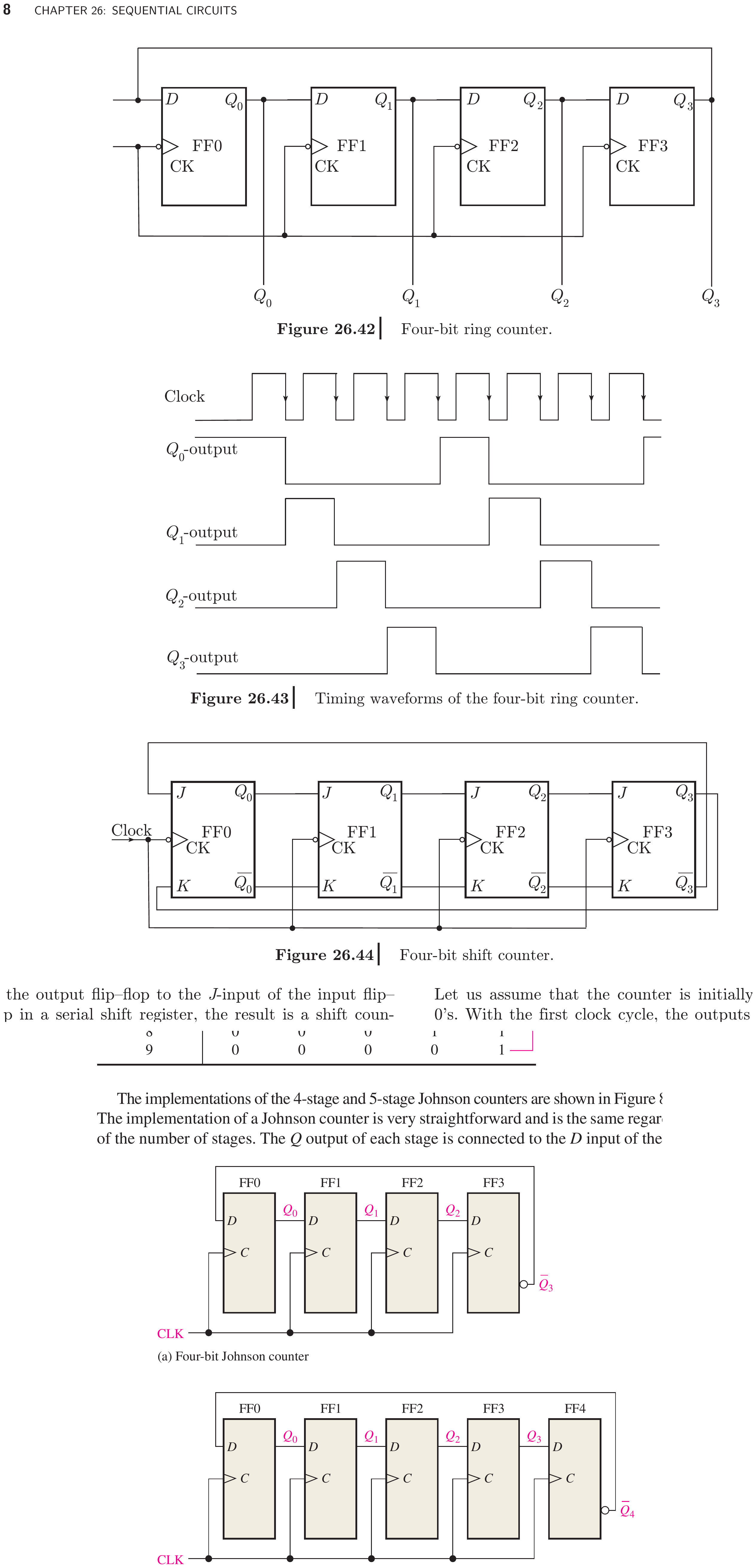
Decoding: Each state is decoded by a single 2-input AND gate (using adjacent FF outputs or their complements).
Ring vs Johnson — Comparison
| Feature | Ring Counter | Johnson Counter |
|---|---|---|
| Feedback | \(Q_{last} \to D_{first}\) (normal) | \(\overline{Q_{last}} \to D_{first}\) (complemented) |
| States for \(n\) FFs | \(n\) | \(2n\) |
| Decoding | Self-decoding (no gates needed) | Simple (2-input AND gates) |
| Efficiency | Low (only \(n\) states from \(n\) FFs) | Better (\(2n\) states from \(n\) FFs) |
| Application | One-hot state machines | Phase generators, timing circuits |
Linear Feedback Shift Register (LFSR)
Definition: An LFSR is a shift register where the input bit is a linear function (XOR) of selected output bits (called taps). It generates a pseudo-random binary sequence (PRBS) with a maximum sequence length of \(2^n - 1\) states (all states except the all-zero state).
Used in: pseudo-random number generation, CRC (cyclic redundancy check) computation, scrambling/descrambling in communication systems, built-in self-test (BIST).
Key Exam Points — Sequence Generators
- Ring counter: \(n\) FFs → \(n\) states, one '1' circulates, self-decoding.
- Johnson counter: \(n\) FFs → \(2n\) states, complemented feedback, simple decoding.
- LFSR: \(n\) FFs → up to \(2^n - 1\) pseudo-random states (XOR feedback).
Model Answer — Shift-Register Types and Applications [5 marks]
Exam-ready answer
A shift register is a group of clocked flip-flops, normally D types, that stores an \(n\)-bit word and moves data by one stage at each active clock edge. All stages share the clock. For the pictured four-stage right-shift convention,
and serial output is taken from \(Q_0\). “Left” and “right” depend on how bits are drawn and numbered, so the update equation or arrow must always be stated.
| Type | Loading | Reading | Main operation/application |
|---|---|---|---|
| SISO | One serial bit per clock | One serial bit from last stage | \(n\)-clock delay, serial transfer |
| SIPO | Serial | All \(n\) outputs together | Serial-to-parallel reception |
| PISO | All \(n\) bits on a load control | One bit per clock | Parallel-to-serial transmission |
| PIPO | All bits together | All bits together | Temporary word storage/buffering |
Shift check: starting at \(0000\) and entering \(1,0,1,1\) at \(D_{in}\) gives \(1000\), \(0100\), \(1010\), then \(1101\). This verifies both stage direction and clock-by-clock storage. A universal register adds multiplexers before each D input to select hold, shift left, shift right or parallel load; the 74194 is a common example.
Registers require setup/hold times and a clean common clock. They store and rearrange bits but do not by themselves interpret a serial protocol. Feedback variants include ring and Johnson counters. An LFSR yields the often-quoted maximum \(2^n-1\) period only for suitable primitive taps and a nonzero seed; an all-zero XOR-feedback state is locked.
Practice target: 8 minutes; draw four D stages, state one unambiguous shift equation and reproduce the four-type table plus the sample sequence.
Model Answer — Two-Bit Asynchronous Ripple Counter [5 marks, PYQ 2082]
Exam-ready answer
A two-bit asynchronous counter uses two toggle stages, implemented by T flip-flops with \(T=1\) or JK flip-flops with \(J=K=1\). Only FF0 receives the external clock. For falling-edge-triggered devices, \(Q_0\) clocks FF1; FF0 toggles at every external falling edge and FF1 toggles at each falling edge of \(Q_0\).
| Applied pulses | \(Q_1Q_0\) | Decimal |
|---|---|---|
| 0 | 00 | 0 |
| 1 | 01 | 1 |
| 2 | 10 | 2 |
| 3 | 11 | 3 |
| 4 | 00 | 0, repeat |
Thus the circuit is a mod-\(2^2=4\) up-counter. \(Q_0\) has frequency \(f_{CLK}/2\) and \(Q_1\) has \(f_{CLK}/4\), so it is also a two-stage frequency divider. With the opposite edge convention, \(Q\) versus \(\overline Q\) clock connections must be selected accordingly; the required test is the state sequence, not a memorised terminal.
It is called “ripple” because the second state change waits for FF0's propagation delay. During \(01\to10\), \(Q_0\) may become 0 before \(Q_1\) becomes 1, momentarily producing \(00\). For \(n\) stages the settling time is roughly \(nt_{pd}\) and a conservative limit is \(f_{max}\lesssim1/(nt_{pd})\). This simplicity suits low-speed counters/dividers, but decoded outputs can glitch and high-speed systems use synchronous counters.
Practice target: 8 minutes; draw the two JK/T stages, label the triggering edge and reproduce the four states with both divided waveforms.
Model Answer — Synchronous and Ripple Counter Comparison [5 marks]
Exam-ready answer
A counter advances through a prescribed state sequence on clock events. In an asynchronous or ripple counter only the least-significant flip-flop receives the external clock; every later stage is triggered by an earlier output. In a synchronous counter every flip-flop receives the same clock edge, and combinational input logic decides which stages toggle.
| Property | Asynchronous (ripple) | Synchronous |
|---|---|---|
| Clock distribution | External clock to first FF only | Common clock to every FF |
| State transition | Propagates stage by stage | All state bits update on one edge |
| Delay | Approximately \(nt_{pd}\) | FF delay plus worst input-logic delay, not cumulative through FFs |
| Decoding | Transitional states can cause glitches | Stable after one common-edge settling interval |
| Hardware | Very simple | Requires excitation/enable logic |
| Speed | Low | High |
| Arbitrary sequence | Awkward, often decoded reset | Natural state-table/K-map design |
| Uses | Frequency dividers, low-speed timers | CPUs, high-speed timers, programmable mod-\(N\) counters |
For a binary synchronous JK up-counter, all flip-flops share CLK; \(J_0=K_0=1\), \(J_1=K_1=Q_0\), and generally bit \(i\) toggles when every lower bit is 1. A ripple counter achieves binary division with almost no gating, but its intermediate transitions matter: for example \(0111\to1000\) may briefly pass through several false codes. Synchronous operation greatly reduces such decoding hazards, though unequal combinational paths can still require proper settling and registered outputs.
Practice target: 8 minutes; reproduce at least six comparison rows and explain one ripple glitch using a multi-bit transition.
Model Answer — Synchronous Mod-5 JK Counter Design [10 marks]
Exam-ready answer
A mod-5 counter requires five states, so the number of flip-flops is
Let the outputs be \(Q_2Q_1Q_0\) and require
All three JK flip-flops receive one common clock. Use the JK excitation rules \(0\to0:J=0\), \(0\to1:J=1\), \(1\to0:K=1\), \(1\to1:K=0\), with the other input a don't-care.
| Present | Next | \(J_2\) | \(K_2\) | \(J_1\) | \(K_1\) | \(J_0\) | \(K_0\) |
|---|---|---|---|---|---|---|---|
| 000 | 001 | 0 | \(\times\) | 0 | \(\times\) | 1 | \(\times\) |
| 001 | 010 | 0 | \(\times\) | 1 | \(\times\) | \(\times\) | 1 |
| 010 | 011 | 0 | \(\times\) | \(\times\) | 0 | 1 | \(\times\) |
| 011 | 100 | 1 | \(\times\) | \(\times\) | 1 | \(\times\) | 1 |
| 100 | 000 | \(\times\) | 1 | 0 | \(\times\) | 0 | \(\times\) |
States 101, 110 and 111 are unused and may be entered as don't-cares for minimisation, followed by an explicit recovery check. The six Karnaugh maps give
Using \(Q^+=J\overline Q+\overline KQ\), the realised next-state equations are
Substitution verifies the legal sequence:
| Present | Computed next |
|---|---|
| 000 | 001 |
| 001 | 010 |
| 010 | 011 |
| 011 | 100 |
| 100 | 000 |
It also proves self-recovery for this particular minimisation: \(101\to010\), \(110\to010\), and \(111\to000\). Thus no unused state traps the counter, although this must be checked rather than assumed from K-map don't-cares.
The circuit is synchronous because all stored bits update only on the common edge; \(Q_0\) does not clock \(Q_1\). A reset should initialise \(000\). The final design should be checked for the five-state period, unused-state recovery, setup time through the input gates and a clock period exceeding combinational plus flip-flop delay.
Practice target: 18 minutes; complete the excitation table, six K-maps, circuit and all eight next-state substitutions.
Model Answer — Ring and Johnson Sequence Generators [5 marks]
Exam-ready answer
A sequence generator is a clocked sequential circuit whose outputs repeat a prescribed pattern. Ring and Johnson counters obtain such patterns by feeding the end of a shift register back to its input.
For a four-stage ring counter, normal last-stage output is fed back and a one-hot seed is loaded:
An \(n\)-stage ring has \(n\) useful states. Each state already has one asserted output, so decoding is immediate, but it uses many flip-flops per state. It must be preset to a one-hot word; all-zero remains all-zero, and multiple-1 patterns form unintended cycles.
For a four-stage Johnson (twisted-ring) counter, the complement of the last output is fed to the first:
An \(n\)-stage Johnson counter has \(2n\) states, and adjacent output combinations allow simple two-input decoding. It is more state-efficient than a ring but still uses only \(2n\) of the possible \(2^n\) states. It is not inherently self-correcting: reset/startup logic or illegal-state correction may be required to prevent an invalid cycle.
| Feature | Ring | Johnson |
|---|---|---|
| Feedback | \(Q_{last}\) | \(\overline{Q_{last}}\) |
| Valid states | \(n\) | \(2n\) |
| Pattern | One-hot circulation | Run of 1s fills, then empties |
| Uses | One-hot timing/control | Multi-phase clocks, sequence timing |
An LFSR is another feedback sequence generator, but its \(2^n-1\) maximum is achieved only with a primitive feedback polynomial and nonzero seed; XOR feedback leaves all-zero locked.
Practice target: 8 minutes; draw both feedback paths and write all four ring and eight Johnson states in the stated direction.