Operational-Amplifier Fundamentals and Parameters
Possible Exam Questions
Exam Questions and Answer Map
Questions marked [PYQ paper/year] were directly observed in past papers; [likely] means pattern-based prediction.
-
List ideal op-amp characteristics and explain virtual short and virtual ground. [5] — [likely]
-
Model answer: Ideal Op-Amp, Virtual Short and Virtual Ground
-
Define and explain the important performance parameters of a practical op-amp. [10] — [likely]
-
Model answer: Practical Op-Amp Performance Parameters
1. Fundamentals and Practical Parameters
Likely Exam Question (10 marks)
"Define an operational amplifier. Explain its ideal characteristics and derive the gain expressions for inverting and non-inverting configurations." OR "Define CMRR and Slew Rate. Why are they important in op-amp applications?"
Definition
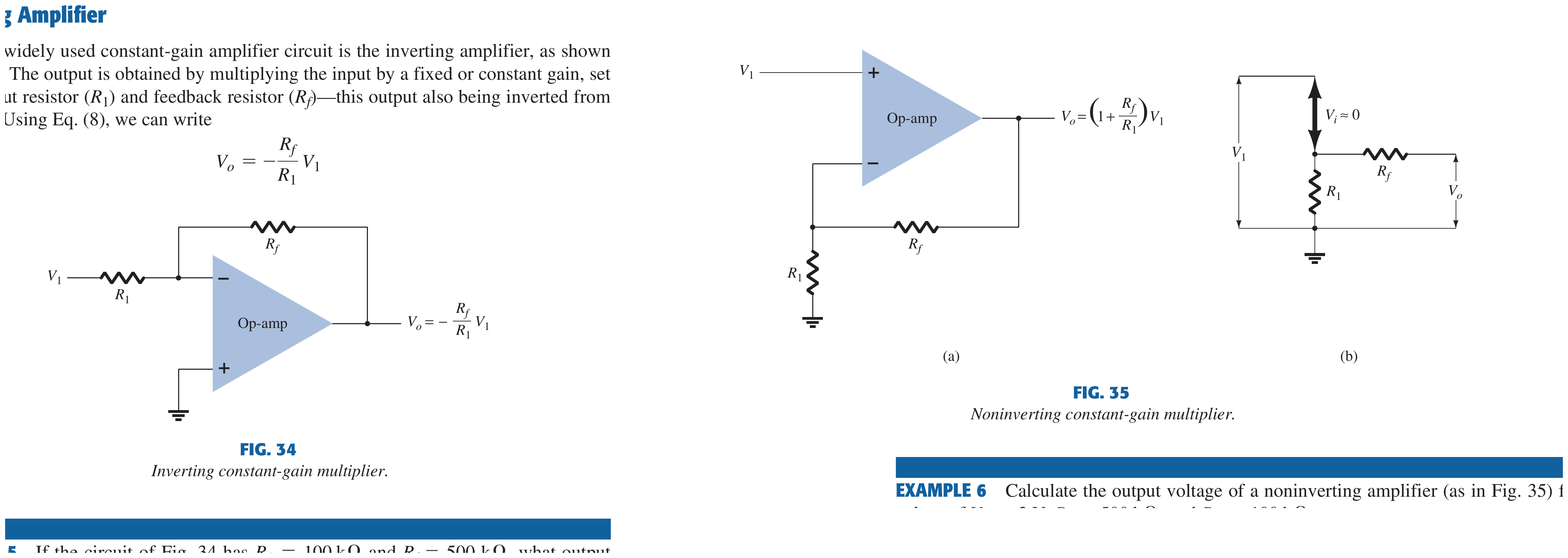
An Operational Amplifier (Op-Amp) is a high-gain, direct-coupled, differential-input, single-ended-output voltage amplifier. It amplifies the difference between the voltages applied at its two inputs (non-inverting \(V^+\) and inverting \(V^-\)):
where \(A_{OL}\) is the open-loop voltage gain. The op-amp is called "operational" because it was originally designed to perform mathematical operations (addition, subtraction, integration, differentiation) in analog computers.
Internal Block Arrangement
Signal flow:
- Differential input stage
- accepts \(V^+\) and \(V^-\);
- provides high input resistance;
- supplies the first differential gain;
- rejects common-mode signals;
- establishes input bias current, offset and noise performance.
- High-gain and level-shift stages
- provide most of \(A_{OL}\);
- convert the internal differential signal toward a single-ended signal;
- shift the DC level for the output stage;
- include dominant-pole compensation for stable feedback operation.
- Class-AB push-pull output stage
- supplies load current in both polarities;
- lowers output resistance;
- increases output-voltage swing;
- limits practical current, swing and short-circuit capability.
The stages are direct coupled, so the op-amp can amplify signals down to DC. Direct coupling also means that input offset and temperature drift propagate to the output.
Ideal vs Practical Op-Amp Characteristics
| Parameter | Ideal Op-Amp | Practical Op-Amp (µA741) |
|---|---|---|
| Open-loop voltage gain (\(A_{OL}\)) | \(\infty\) | \(\sim 2 \times 10^5\) (106 dB) |
| Input impedance (\(Z_{in}\)) | \(\infty\) | \(\sim 2\,\text{M}\Omega\) |
| Output impedance (\(Z_{out}\)) | \(0\) | \(\sim 75\,\Omega\) |
| Bandwidth | \(\infty\) | \(\sim 1\,\text{MHz}\) (unity-gain BW) |
| Common Mode Rejection Ratio (CMRR) | \(\infty\) | \(\sim 90\,\text{dB}\) |
| Slew Rate | \(\infty\) | \(0.5\,\text{V/}\mu\text{s}\) |
| Input offset voltage | \(0\) | \(\sim 1\,\text{mV}\) |
| Input bias current | \(0\) | \(\sim 80\,\text{nA}\) |
| Input offset current | \(0\) | \(\sim 20\,\text{nA}\) |
Practical Equivalent Model
The low-frequency voltage model contains:
- Differential input resistance \(R_i\): connected between the two inputs; it is large but finite, so practical input currents are not exactly zero.
- Controlled voltage source: produces the internal voltage \(A_{OL}V_d\), where \(V_d=V^+-V^-\).
- Output resistance \(R_o\): appears in series with the controlled source; negative feedback reduces the effective closed-loop output resistance.
- Frequency dependence: \(A_{OL}\) is not constant; internal capacitances make it fall with frequency.
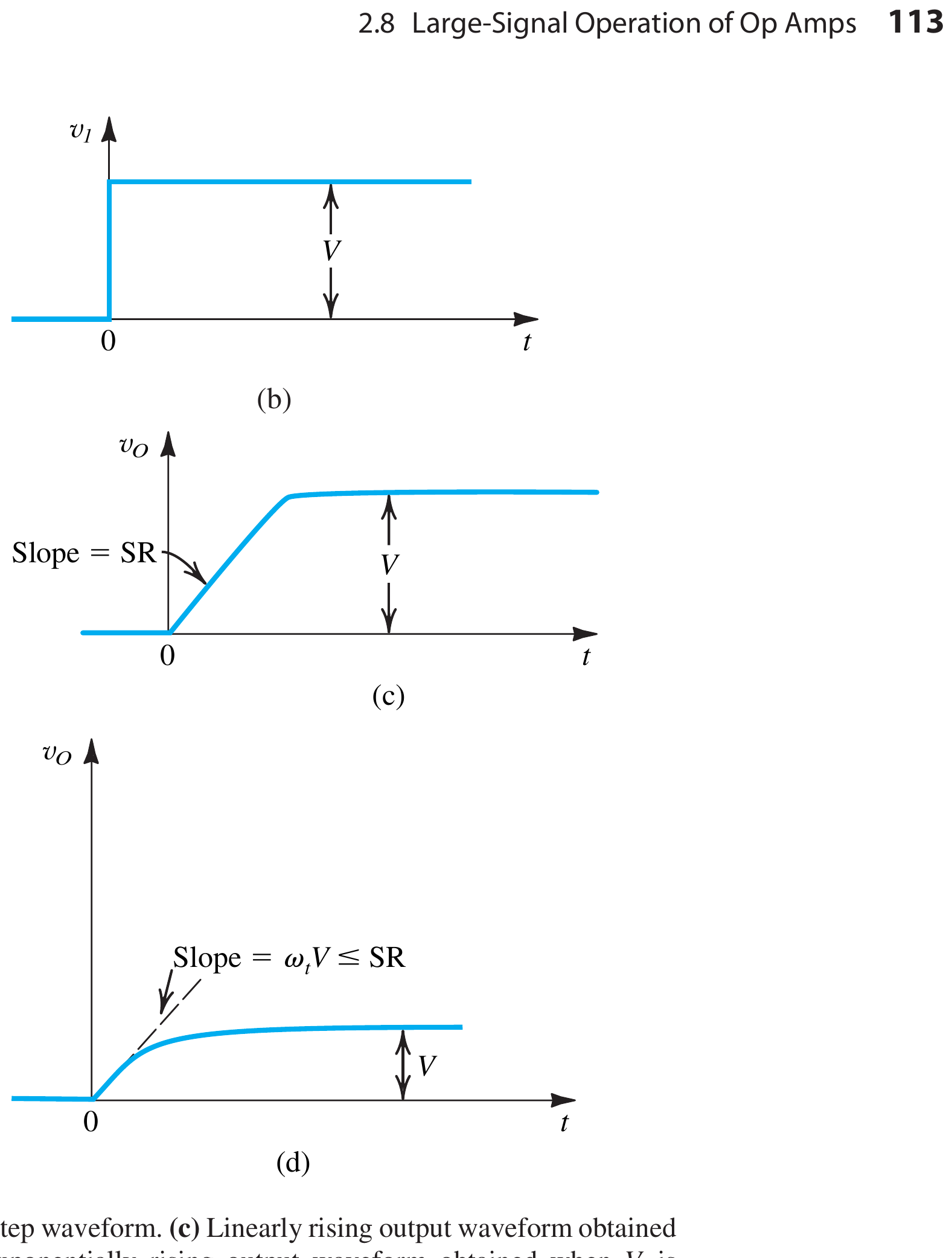
- Large-signal limit: even inside small-signal bandwidth, output slope cannot exceed the slew rate.
The ideal model follows from the limits
Key Op-Amp Parameters
Common Mode Rejection Ratio (CMRR):
CMRR is defined as the ratio of the differential-mode gain (\(A_d\)) to the common-mode gain (\(A_{cm}\)):
An ideal op-amp has infinite CMRR — it completely rejects signals that are common to both inputs (such as noise, interference, hum) and amplifies only the difference signal. High CMRR is essential in instrumentation amplifiers measuring small differential signals in noisy environments.
Slew Rate (SR):
Slew Rate is defined as the maximum rate of change of output voltage with respect to time:
The slew rate limits the maximum frequency at which the op-amp can produce undistorted full-amplitude output (full-power bandwidth):
where \(V_p\) is the peak output voltage. Above this frequency, the output becomes a triangular wave instead of a sinusoid.
For µA741: \(SR = 0.5\,\text{V/}\mu\text{s}\). For \(V_p = 10\,\text{V}\): \(f_{\max} = \frac{0.5 \times 10^6}{2\pi \times 10} = 7.96\,\text{kHz}\).
Virtual Short / Virtual Ground Principle:
In a negative-feedback op-amp circuit, two key assumptions hold:
- No current flows into the op-amp inputs: \(I^+ = I^- = 0\) (infinite input impedance)
- Both inputs are at the same voltage: \(V^+ = V^-\) (infinite gain forces the differential input to zero)
When the non-inverting input is grounded, the inverting input is at virtual ground (\(V^- \approx 0\)).
Frequency Response and Gain-Bandwidth Product
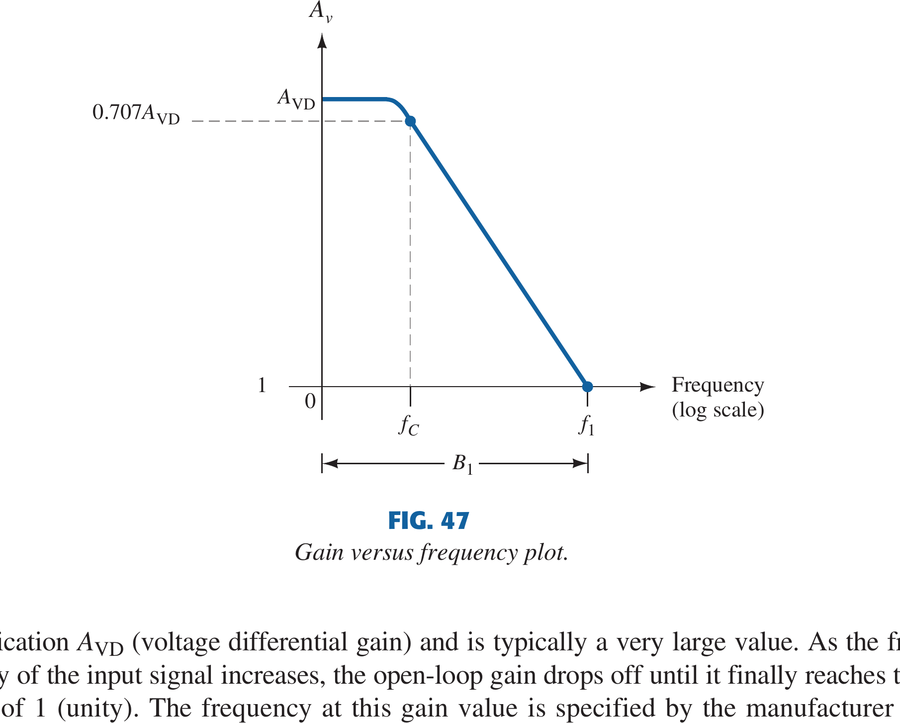
For a dominant-pole compensated op-amp,
Key points:
- \(A_0\) is very large at low frequency.
- At the dominant pole \(f_p\), magnitude is \(3\) dB below \(A_0\).
- Above \(f_p\), open-loop gain falls at approximately \(20\) dB/decade.
- The transition or unity-gain frequency \(f_T\) is where \(|A_{OL}|=1\) or \(0\) dB.
-
For a single dominant pole,
\[ \boxed{GBW\approx A_0f_p\approx f_T}. \] -
Negative feedback trades gain for bandwidth. For closed-loop noise gain \(A_N\),
\[ \boxed{BW\approx\frac{f_T}{A_N}}. \] -
The familiar \(A_{CL}\times BW\approx f_T\) form applies when the relevant closed-loop gain equals the noise gain.
Small-Signal Bandwidth vs Full-Power Bandwidth
- Small-signal bandwidth: set mainly by poles and gain-bandwidth product; the output remains in its linear small-signal regime.
-
Full-power bandwidth: set by slew rate for a required peak output \(V_p\):
\[ \boxed{f_{FP}=\frac{SR}{2\pi V_p}}. \] -
The usable maximum frequency is the lower limit imposed by small-signal response, slew rate, output swing and output-current capability.
Practical Performance Parameters
| Parameter | Definition or key relation | Ideal value | Why it matters |
|---|---|---|---|
| Open-loop gain \(A_{OL}\) | \(V_o/(V^+-V^-)\) without feedback | \(\infty\) | Determines loop gain and closed-loop accuracy |
| Input impedance \(Z_i\) | Impedance seen between/at input terminals | \(\infty\) | High \(Z_i\) minimizes source loading |
| Output impedance \(Z_o\) | Small-signal impedance looking into output | \(0\) | Low \(Z_o\) gives load-independent voltage |
| CMRR | \(\lvert A_d/A_{cm}\rvert\) | \(\infty\) | Rejects equal interference on both inputs |
| PSRR | Rejection of supply change, commonly \(\lvert\Delta V_S/\Delta V_{OS}\rvert\) | \(\infty\) | Prevents supply ripple/drift becoming signal error |
| GBW or \(f_T\) | Approximately \(A_{CL}\times BW\) for a dominant-pole case | \(\infty\) | Limits small-signal closed-loop speed |
| Slew rate | \(\max\lvert dV_o/dt\rvert\) | \(\infty\) | Limits large-amplitude high-frequency output |
| Settling time \(t_s\) | Time to enter and stay inside a specified error band | \(0\) | Limits conversion and acquisition speed |
| Input offset voltage \(V_{OS}\) | Differential input needed to force \(V_o=0\) | \(0\) | Produces DC output error multiplied by noise gain |
| Input bias current \(I_B\) | Average of the two input currents | \(0\) | Creates source-resistance voltage drops |
| Input offset current \(I_{OS}\) | Magnitude of input-current mismatch | \(0\) | Leaves error even with resistance balancing |
| Drift | Parameter change per degree or time | \(0\) | Controls long-term and temperature accuracy |
Power-Supply Rejection Ratio
Using the input-referred offset-change convention,
- Higher PSRR is better.
- Some data sheets instead specify supply sensitivity \(\Delta V_{OS}/\Delta V_S\) in \(\mu\text{V}/\text{V}\); then a smaller number is better.
- PSRR generally worsens as frequency rises, so supply decoupling remains necessary.
Input and Output Impedance
- Differential input impedance is measured between \(V^+\) and \(V^-\).
- Common-mode input impedance is measured from tied inputs to ground.
- FET/CMOS-input op-amps have very small bias current and very high DC input resistance.
- Negative voltage feedback usually raises effective input impedance for a non-inverting connection and lowers closed-loop output impedance.
- Practical output impedance rises at high frequency as loop gain falls.
Settling Time
After a step input, output response may contain:
- Slew interval: output moves at its maximum slope.
- Linear settling interval: small-signal response approaches final value.
- Ringing: insufficient phase margin may cause overshoot before the output stays inside the tolerance band.
Settling time must always state the error band, for example \(0.1\%\), \(0.01\%\) or a number of LSBs.
Offsets, Bias Currents and Drift
Input bias and offset currents are
- \(V_{OS}\) is modeled as a small DC source in series with one input.
- With both external inputs grounded, \(V_{OS}\) and bias-current drops create output offset voltage.
- Input offset error is multiplied approximately by circuit noise gain, not always by signal gain.
- Matching the DC resistance seen by both inputs reduces average bias-current error but not \(I_{OS}\) error.
- Offset drift is commonly specified in \(\mu\text{V}/^\circ\text{C}\) and bias-current drift in \(\text{pA}/^\circ\text{C}\) or \(\text{nA}/^\circ\text{C}\).
How to Score a Parameter Question
For every requested parameter, write **full name → definition/formula → ideal value/unit → one practical effect**. Do not submit only a list of abbreviations.
Model Answer — Ideal Op-Amp, Virtual Short and Virtual Ground [5 marks]
Exam-ready answer
An operational amplifier is a direct-coupled, very-high-gain differential voltage amplifier with two inputs and one output:
where \(A_{OL}\) is open-loop gain, \(V^+\) the non-inverting input and \(V^-\) the inverting input.
Ideal characteristics:
| Parameter | Ideal value | Consequence |
|---|---|---|
| Open-loop differential gain \(A_{OL}\) | \(\infty\) | Tiny differential input can control finite output |
| Input resistance \(R_{in}\) | \(\infty\) | \(i^+=i^-=0\); source is not loaded |
| Output resistance \(R_o\) | \(0\) | Output voltage is independent of load |
| Bandwidth and slew rate | \(\infty\) | No frequency or large-signal speed limit |
| CMRR and PSRR | \(\infty\) | Perfect rejection of common-mode and supply variations |
| Offset voltage, bias/offset currents and noise | \(0\) | Zero output for equal inputs |
Virtual short: with negative feedback, linear operation and an unsaturated output, \(A_{OL}\) is extremely large but \(V_o\) is finite. Therefore
The inputs are equal in voltage but are not physically shorted; because \(R_{in}\to\infty\), no current flows between or into them.
Virtual ground: if negative feedback holds and \(V^+\) is connected to actual ground, the virtual-short condition makes \(V^-\approx0\,\text{V}\). This node is called a virtual ground. It has ground potential but no direct ground connection and cannot independently source or sink load current; currents entering it must flow through the external feedback network.
These rules do not apply in open-loop comparator operation, positive feedback, or when the output is saturated. They are the basis of closed-loop op-amp gain derivations.
Practice target: 8–9 minutes; list the ideal properties and state all three conditions required for a virtual short.
Model Answer — Practical Op-Amp Performance Parameters [10 marks]
Exam-ready answer
A practical op-amp is modeled by finite differential input resistance \(R_i\), a frequency-dependent controlled source \(A_{OL}V_d\) and non-zero output resistance \(R_o\).
Important parameters:
-
Open-loop gain:
$$ A_{OL}=\frac{V_o}{V^+-V^-} $$
without feedback. Large \(A_{OL}\) gives high loop gain and accurate closed-loop gain, but it falls with frequency.
-
Input impedance \(Z_i\): impedance seen by the signal source. It should be high to minimize loading and input current.
- Output impedance \(Z_o\): impedance looking into the output. It should be low so load current causes little output-voltage change.
-
Bandwidth and gain-bandwidth product: a dominant-pole op-amp rolls off at about \(20\) dB/decade and has unity-gain frequency \(f_T\). Approximately,
$$ \boxed{A_N\times BW\approx f_T}. $$
-
Slew rate: maximum large-signal output slope,
$$ \boxed{SR=\max\left|\frac{dV_o}{dt}\right|}, \qquad \boxed{f_{FP}=\frac{SR}{2\pi V_p}}. $$
-
CMRR:
$$ \boxed{\mathrm{CMRR}=\left|\frac{A_d}{A_{cm}}\right|}, \qquad \mathrm{CMRR}{dB}=20\log). $$}(\mathrm{CMRR
High CMRR rejects interference common to both inputs.
-
PSRR: measures rejection of supply change. With the input-referred convention,
$$ \boxed{\mathrm{PSRR}=\left|\frac{\Delta V_S}{\Delta V_{OS}}\right|}. $$
-
Input offset voltage \(V_{OS}\): small differential DC voltage required for zero output. It produces output error multiplied by noise gain.
-
Input currents:
$$ I_B=\frac{|I_{B+}|+|I_{B-}|}{2}, \qquad I_{OS}=\left||I_{B+}|-|I_{B-}|\right|. $$
They create errors across source resistances.
-
Settling time: time after a step for output to enter and remain within a stated error band. It includes slew, linear settling and possible ringing.
- Drift: change of offset or current with temperature/time; low drift is essential in precision DC systems.
Bandwidth is a small-signal pole limit, slew rate is a large-signal slope limit, and settling time includes both plus transient accuracy. A complete specification also checks input common-mode range, output swing/current, noise and stability.
Practice target: 18 minutes; for each parameter write its full name, definition or formula, ideal direction and one circuit consequence.