CE RC-Coupled Amplifier
Possible Exam Questions
Exam Questions and Answer Map
-
Draw and explain a CE RC-coupled amplifier. Derive its gains and explain its frequency response. [10] — [likely]
-
Answer plan: Draw bias and signal path → explain DC Q point and alternating collector current → derive \(A_v\), distinguish intrinsic and overall \(A_i\), state \(A_p\) → explain low/mid/high regions, \(f_L\), \(f_H\), bandwidth and Miller effect.
- Model answer: CE RC-Coupled Amplifier and Frequency Response
1. Complete Circuit
A common-emitter (CE) RC-coupled stage uses a BJT biased in the active region, resistive collector and emitter networks, and capacitors to couple the signal without disturbing DC bias.
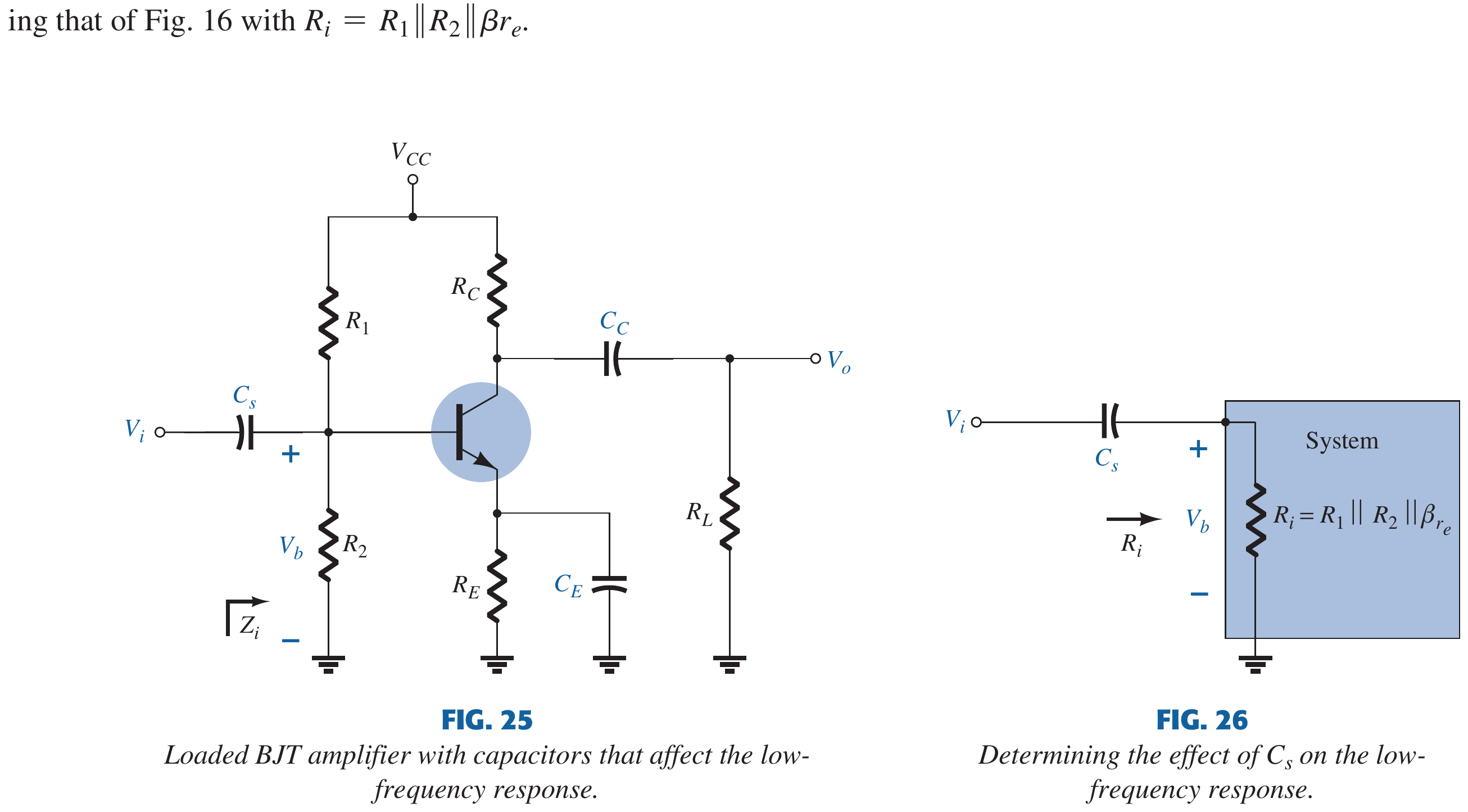
Function of Each Component
| Component | Function |
|---|---|
| \(R_1,R_2\) | Voltage-divider bias for a stable base voltage |
| \(R_C\) | Converts collector-current change into output-voltage change |
| \(R_E\) | DC negative feedback that stabilises emitter/collector current |
| \(C_E\) | Bypasses \(R_E\) for AC in the intended band, increasing gain |
| \(C_i\) | Couples source AC to the base while blocking source/amplifier DC |
| \(C_o\) | Couples collector AC to \(R_L\) while blocking collector DC |
| \(R_L\) | External load receiving output signal power |
2. DC Bias and Q Point
At DC, \(C_i\), \(C_o\) and \(C_E\) are open. The approximate divider voltage and emitter current are
The Q point must keep \(Q_1\) in the active region and permit approximately symmetrical collector-voltage swing without cutoff or saturation.
3. AC Working Principle
Positive Input Half-Cycle
- \(v_{BE}\) and base current increase.
- Collector current \(i_C\) increases.
- Drop \(i_CR_C\) increases.
- Collector voltage \(v_C=V_{CC}-i_CR_C\) decreases.
Negative Input Half-Cycle
- Base and collector currents decrease.
- The drop across \(R_C\) decreases.
- Collector voltage rises.
Thus output voltage is amplified and \(180^\circ\) out of phase with input. The transistor controls DC-supply power; the input merely controls that process.
4. Midband Small-Signal Gains
At room temperature,
If \(C_E\) effectively bypasses \(R_E\), transistor output resistance is neglected, and \(R_C'=R_C\parallel R_L\),
Without effective emitter bypass, local feedback lowers gain approximately to
under the usual simplified model.
The transistor's intrinsic current gain is
The overall load current gain \(A_i=i_o/i_i\) need not equal \(\beta_{ac}\) because \(R_1\parallel R_2\), source resistance and load division carry some current. Once port currents are defined,
for sinusoidal resistive port quantities.
Loading Check
when transistor output resistance is large. A finite source resistance attenuates the applied signal before it reaches the base, and \(R_L\) lowers \(R_C'\), so measured gain is less than an unloaded intrinsic estimate.
5. Three-Region Frequency Response
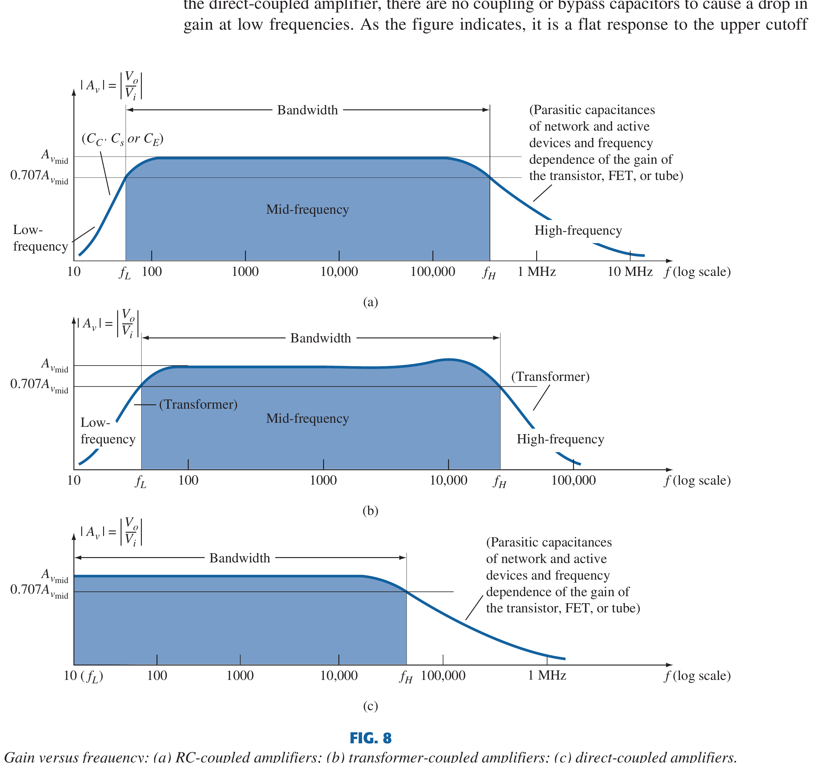
Low-Frequency Region
At low \(f\), capacitor reactance \(X_C=1/(2\pi fC)\) is large:
- \(C_i\) attenuates the base signal;
- \(C_o\) attenuates transfer to \(R_L\);
- \(C_E\) incompletely bypasses \(R_E\), increasing emitter degeneration.
Each creates a high-pass pole. For example, a first estimate for the input-coupling pole is
The actual \(f_L\) is the combined response of all low-frequency poles, not automatically the largest single estimate when poles are close.
Midband Region
\(C_i\), \(C_o\) and \(C_E\) act approximately as shorts for signal, while device capacitances act approximately as opens. Gain is nearly constant at \(A_{v(mid)}\).
High-Frequency Region
Base-emitter diffusion capacitance \(C_\pi\), base-collector capacitance \(C_\mu\), wiring capacitance and load capacitance shunt signal and reduce gain. The most important multiplication mechanism in a high-gain CE stage is the Miller effect.
How the Miller Effect Works
\(C_\mu\) bridges the input base and output collector rather than connecting either node directly to ground. If the stage voltage gain is \(A_v=v_o/v_i\), the capacitor current is
The source must therefore supply the same current that would flow through an input-to-ground capacitance
The last form applies because a CE amplifier is inverting, so \(A_v<0\). A small positive base change makes the collector change in the opposite direction; hence the voltage change across \(C_\mu\) is approximately \((1+\lvert A_v\rvert)\) times the input change. The physical capacitor has not increased: feedback through the moving output makes it appear larger at the input.
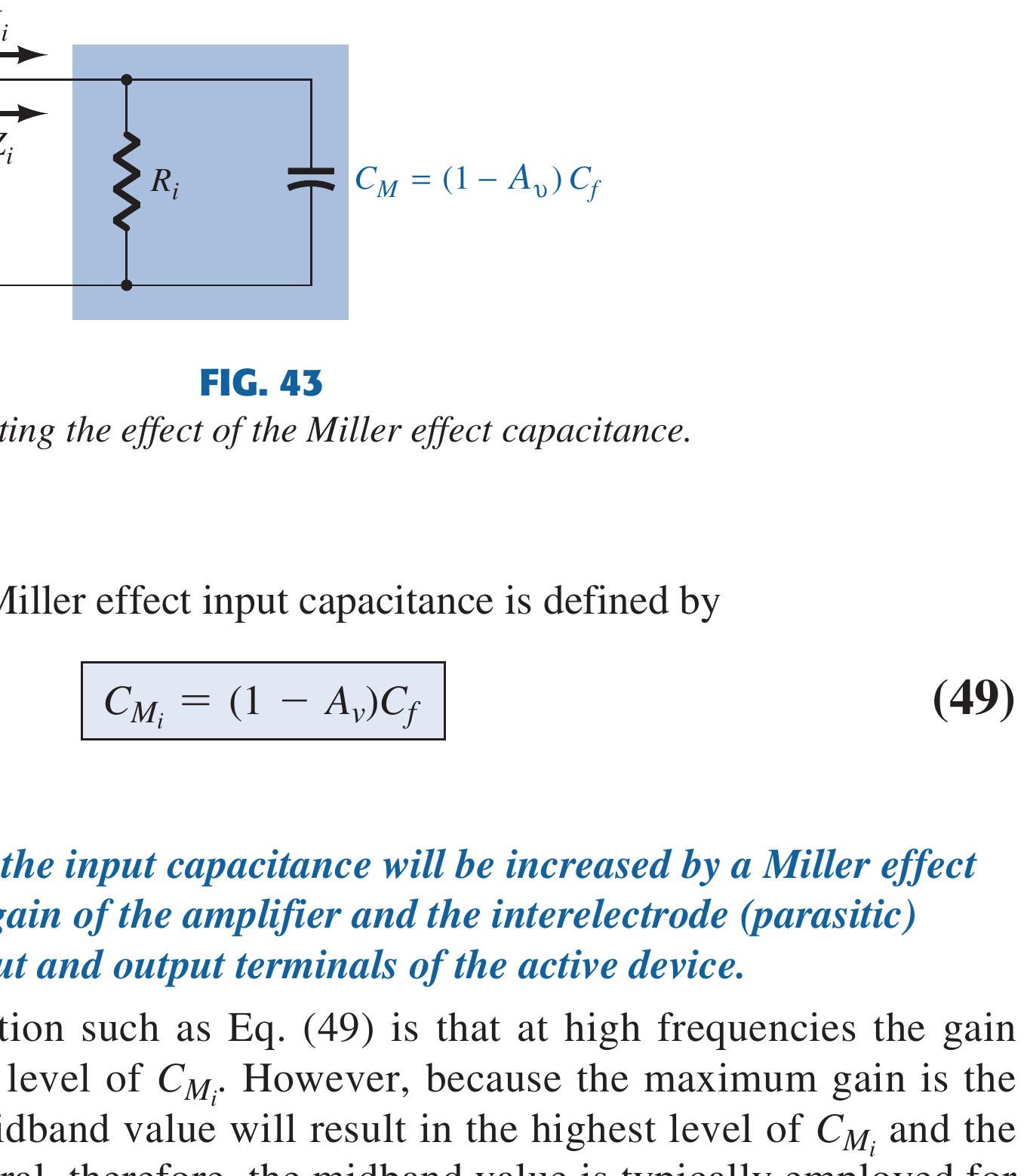
Miller's theorem replaces the bridging capacitor by two grounded equivalents:
For large negative gain, \(C_{Mi}\approx C_\mu(1+\lvert A_v\rvert)\) can be much larger than \(C_\mu\), whereas \(C_{Mo}\approx C_\mu\). The approximate total input capacitance is therefore
where \(C_{wi}\) represents input wiring and stray capacitance.
Effect on Circuit Performance
- Lower input impedance at high frequency: \(X_{C_{Hi}}=1/(2\pi fC_{Hi})\) falls as frequency rises, so more source current is diverted through capacitance.
- Lower upper cutoff and bandwidth: with \(R_{Hi}\) equal to the resistance seen by the input capacitance,
$$ f_{Hi}\approx\frac{1}{2\pi R_{Hi}C_{Hi}}, \qquad R_{Hi}\approx R_s\parallel R_1\parallel R_2\parallel r_\pi. $$
Miller multiplication increases \(C_{Hi}\) and can make this the dominant high-frequency pole, thereby lowering \(f_H\). - High-frequency gain loss: increasing capacitive current attenuates the base signal, so voltage gain rolls off above the pole. - Slower transient response: for an approximately single-pole stage, rise time is \(t_r\approx0.35/f_H\); a lower \(f_H\) therefore means slower response to rapid input changes. - Additional phase lag: the high-frequency poles increase phase shift and can reduce phase margin when the amplifier is enclosed in a feedback loop. - Gain-bandwidth trade-off: increasing \(\lvert A_v\rvert\) strengthens Miller multiplication, so obtaining large gain from one CE stage generally costs bandwidth.
Ways to Reduce or Mitigate It
- Use a cascode: a common-base transistor above the input CE transistor holds its collector at nearly constant AC voltage. The voltage gain across the input transistor's \(C_\mu\) is then small, so Miller multiplication is strongly suppressed. This is the standard wideband solution.
- Use a transistor with small \(C_\mu\): high-frequency devices specify low collector-base feedback capacitance. Short layout traces also reduce wiring capacitance, although they do not alter the multiplication factor.
- Reduce gain per stage: emitter degeneration or distributing the required gain over several lower-gain stages reduces the \((1+\lvert A_v\rvert)\) factor of each stage. The poles of all stages must still be considered.
- Neutralise the feedback capacitance: an added network supplies an equal and opposite high-frequency current. Neutralisation is useful in tuned/RF amplifiers but is frequency-sensitive and poor adjustment can cause instability.
- Use a low-resistance drive or an input buffer: lowering \(R_{Hi}\) raises the input pole. This mitigates the bandwidth loss but does not reduce the Miller-equivalent capacitance itself.
Exam Distinction
Cascode action, lower \(C_\mu\), lower stage gain and neutralisation reduce the Miller mechanism. Lower source resistance only reduces its effect on the pole. Do not write that Miller effect physically changes the capacitor value.
6. Cutoffs and Bandwidth
At either cutoff,
which is \(-3\,\text{dB}\) in voltage gain and half the midband output power for the same load.
For a wideband amplifier with \(f_H\gg f_L\), \(BW\approx f_H\), but the exact definition remains \(f_H-f_L\).
7. Advantages, Disadvantages and Applications
Advantages
- simple, low-cost and compact;
- good midband voltage gain;
- independent DC bias between cascaded stages;
- broad audio/small-signal response;
- no transformer hum, weight or core distortion.
Disadvantages
- gain falls below \(f_L\) and above \(f_H\);
- poor impedance matching and power transfer to low-resistance loads;
- high gain can worsen Miller-limited bandwidth;
- multiple stages load one another and require careful bias/headroom design.
Applications
Audio preamplifiers, microphone and sensor stages, IF/baseband voltage stages, measurement front ends and general-purpose transistor amplification.
Exam Traps
- Midband gain is \(-g_m(R_C\parallel R_L)\) under stated assumptions, not always \(-g_mR_C\).
- \(i_c/i_b\approx\beta_{ac}\) is intrinsic; overall load current gain depends on the whole network.
- \(C_E\) improves AC gain but \(R_E\) must still stabilise DC bias.
- A \(-3\) dB voltage ratio is \(0.707\), not \(0.5\); power is \(0.5\).
Rapid Recall
- Positive base swing → higher \(i_C\) → lower collector voltage.
- \(A_v<0\): CE inversion.
- \(f_L\): coupling/bypass capacitors.
- \(f_H\): device/stray capacitances and Miller effect.
- \(BW=f_H-f_L\).
Model Answer — CE RC-Coupled Amplifier and Frequency Response [10 marks]
Exam-ready answer
A CE RC-coupled amplifier is an untuned small-signal voltage stage. \(R_1,R_2\) establish base bias, \(R_E\) stabilises DC current, \(R_C\) converts collector-current change to voltage, \(C_i,C_o\) block DC while coupling AC, and \(C_E\) bypasses \(R_E\) for AC gain.
At DC the capacitors are open. The divider sets \(V_B\), with \(V_E\approx V_B-V_{BE}\) and \(I_E\approx V_E/R_E\). The Q point is chosen for active-region operation and approximately symmetrical output swing.
On a positive input half-cycle, base and collector currents rise. The \(i_CR_C\) drop rises, so collector voltage falls. On a negative half-cycle the reverse occurs. Hence the output is amplified and inverted by \(180^\circ\).
At midband, if \(C_E\) bypasses \(R_E\) and transistor output resistance is neglected,
The intrinsic transistor current gain is \(i_c/i_b\approx\beta_{ac}\), while overall \(A_i=i_o/i_i\) also depends on the bias, source and load networks. For defined sinusoidal resistive ports, \(A_p=\lvert A_v\rvert A_i\).
At low frequency, \(X_C=1/(2\pi fC)\) is large: \(C_i\) and \(C_o\) attenuate coupling, while incomplete \(C_E\) bypass adds emitter degeneration. Gain therefore rises toward midband. In midband these capacitors are approximately short circuits and device capacitances approximately open, giving nearly constant gain. At high frequency, \(C_\pi\), \(C_\mu\), wiring and load capacitance shunt signal. The inverting gain multiplies base-collector capacitance at the input:
so Miller effect often lowers \(f_H\).
At \(f_L\) and \(f_H\), gain is \(0.707\) of midband or \(-3\) dB; therefore
Advantages are low cost, compact size, independent stage bias and useful broadband voltage gain. Limitations are low/high-frequency roll-off, poor low-load power matching and Miller-limited high-frequency response. It is used in audio preamplifiers, sensors and instrumentation.
Practice target: 18 minutes; draw every bias/coupling component, trace both half-cycles, derive the three gains and label \(f_L\), midband, \(f_H\) and \(BW\) on the response.