MOSFET Switching Characteristics
Possible Exam Questions
Exam Questions and Answer Map
Questions marked [PYQ paper/year] were directly observed in past papers; [likely] means pattern-based prediction.
-
Explain the V-I (drain) characteristics of a MOSFET. [5] — [PYQ 2079]
-
Answer plan: Draw the \(I_D\)–\(V_{DS}\) family → identify cutoff, triode and saturation → mark the pinch-off locus → give the saturation-current equation.
-
Model answer: MOSFET Drain Characteristics
-
Compare BJT and MOSFET switching characteristics. [10] — [likely]
-
Answer plan: Compare control, input impedance, switching mechanism, dominant delay, conduction loss, thermal behaviour and integration density.
- Model answer: BJT and MOSFET Switching Comparison
2. MOS Transistor Switching Characteristics
Likely Exam Questions
"Compare switching characteristics of MOSFET and BJT." OR "Explain why MOSFET switches faster than BJT."
Definition
A MOSFET (Metal-Oxide-Semiconductor Field-Effect Transistor) is a voltage-controlled, three-terminal (Gate, Drain, Source) semiconductor device. As a switch, the MOSFET is controlled by the gate-source voltage \(V_{GS}\). When \(V_{GS}\) exceeds the threshold voltage \(V_{th}\), a conducting channel is formed between drain and source (ON state). When \(V_{GS} < V_{th}\), no channel exists (OFF state). Unlike BJTs, MOSFETs are majority-carrier devices — there is no minority carrier storage, which gives them inherently faster switching speeds.
BJT vs FET — General Device Comparison
Likely Exam Question (5 marks)
"Compare BJT and FET devices."
Both BJTs and FETs are three-terminal semiconductor devices, but they differ fundamentally in how they are controlled and in how current flows through them.
| Parameter | BJT (Bipolar Junction Transistor) | FET (Field-Effect Transistor) |
|---|---|---|
| Control type | Current-controlled | Voltage-controlled |
| Controlling relation | Input current \(I_B\) controls output current \(I_C\) | Input voltage \(V_{GS}\) controls output current \(I_D\) |
| Carrier polarity | Bipolar — both electrons and holes carry current | Unipolar — only one carrier type carries current |
| Current carriers | Majority and minority carriers | Majority carriers only (electrons in N-channel, holes in P-channel) |
| Input impedance | Low (~100 Ω to < 1 MΩ) | Very high (several hundred MΩ) |
| Temperature stability | Less stable (thermal-runaway prone) | More temperature stable |
| Size / integration | Larger | Smaller → extensively used in IC/VLSI fabrication |
| Amplifier gain | Higher gain; better sensitivity to input signal | Lower gain; poorer sensitivity to input signal |
| Handling | More rugged | More sensitive to handling (ESD-prone) |
| Terminals | Base (B), Collector (C), Emitter (E) | Gate (G), Drain (D), Source (S) |
Key point: A BJT is current-controlled and bipolar, whereas a FET is voltage-controlled and unipolar with very high input impedance. Because input impedance is critical in linear AC amplifier design — and because FETs are smaller and more temperature-stable — FETs dominate integrated-circuit fabrication, while BJTs offer higher gain.
MOSFET Types
| Type | Channel | Condition to Turn ON | Default State |
|---|---|---|---|
| Enhancement NMOS | N-type | \(V_{GS} > +V_{th}\) | OFF (no channel exists) |
| Enhancement PMOS | P-type | \(V_{GS} < -\lvert V_{th}\rvert\) | OFF (no channel exists) |
| Depletion NMOS | N-type | ON by default; \(V_{GS} < -\lvert V_P\rvert\) to turn OFF | ON (channel pre-exists) |
| Depletion PMOS | P-type | ON by default; \(V_{GS} > +\lvert V_P\rvert\) to turn OFF | ON (channel pre-exists) |
Enhancement-mode MOSFETs are used in digital circuits (CMOS logic). Depletion-mode MOSFETs are used in analog circuits and as load devices in NMOS logic.
Operating Regions (Enhancement NMOS)
| Region | Condition | Behaviour | Use in Switching |
|---|---|---|---|
| Cutoff | \(V_{GS} < V_{th}\) | No channel; \(I_D \approx 0\) | OFF state (open switch) |
| Triode (Linear) | \(V_{GS} > V_{th}\) and \(V_{DS} < (V_{GS} - V_{th})\) | Channel exists; MOSFET acts as a voltage-controlled resistor with \(R_{DS(on)}\) | ON state (closed switch) |
| Saturation | \(V_{GS} > V_{th}\) and \(V_{DS} \geq (V_{GS} - V_{th})\) | Channel pinched off; \(I_D = \tfrac{1}{2}\mu_n C_{ox}\tfrac{W}{L}(V_{GS} - V_{th})^2\) | Transition region / amplifier use |
When used as a digital switch, the MOSFET operates in cutoff (OFF) and triode (ON). The saturation region is the transition zone during switching.
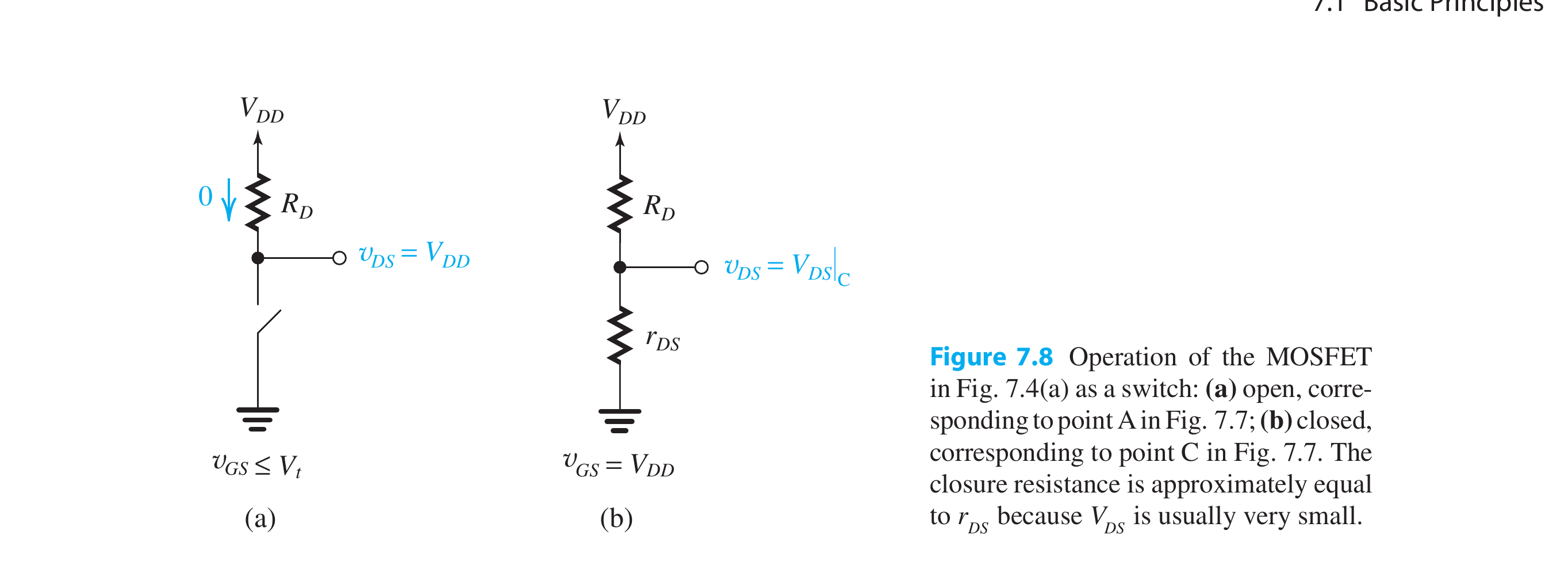
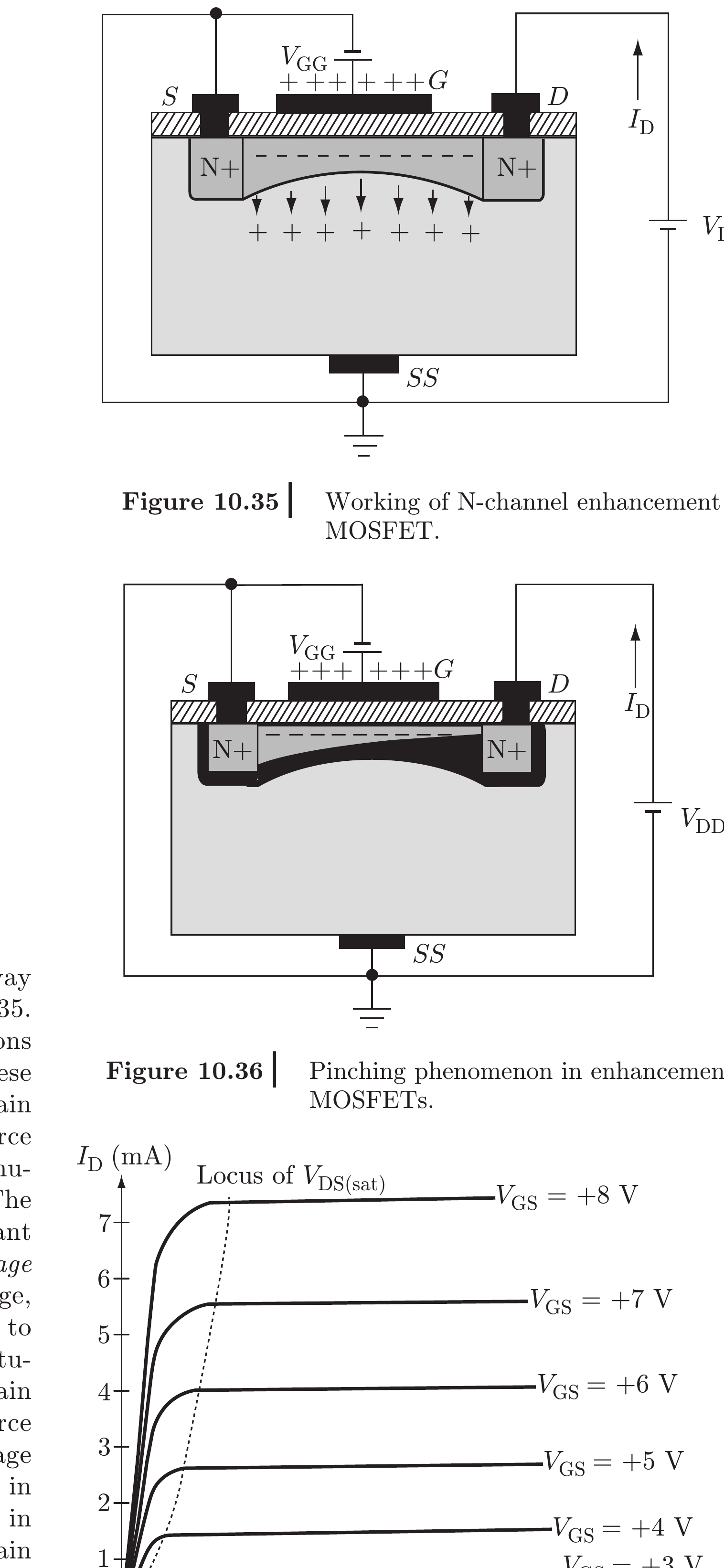

Book-grounded switch interpretation
- OFF: \(V_{GS}<V_{th}\), \(I_D\approx0\), so the drain rises to \(V_{DD}\).
- ON: sufficient gate overdrive moves the device to the low-\(V_{DS}\) ohmic endpoint, where \(V_{DS(on)}\approx I_DR_{DS(on)}\).
- During a transition the operating point can pass through saturation, but the desired steady ON state is deep triode, not saturation.
Source figure: Sedra/Smith, Microelectronic Circuits (7th ed.), PDF p. 410.
Drain characteristics: for each \(V_{GS}\) the device rises through the triode/ohmic region then flattens in saturation beyond the pinch-off boundary \(V_{DS}=V_{GS}-V_{th}\) (dashed). A switch moves between cutoff and deep triode.
Model Answer — MOSFET Drain Characteristics [5 marks, NTC 2079]
Exam-ready answer
An enhancement n-channel MOSFET is a voltage-controlled majority-carrier device. Its drain characteristics are a family of \(I_D\) versus \(V_{DS}\) curves drawn for increasing values of \(V_{GS}\).
- Cutoff: for \(V_{GS}<V_{th}\), no inversion channel exists and \(I_D\approx0\). The device behaves as an open switch.
- Triode or ohmic region: for \(V_{GS}>V_{th}\) and \(0\le V_{DS}<V_{GS}-V_{th}\), a channel exists and
For small \(V_{DS}\) the MOSFET behaves approximately as a voltage-controlled resistance; this is the ON region used in switching.
- Pinch-off boundary: at \(V_{DS}=V_{GS}-V_{th}\), the channel pinches off near the drain.
- Saturation: for \(V_{DS}\ge V_{GS}-V_{th}\), the ideal drain current is nearly independent of \(V_{DS}\):
Increasing \(V_{GS}\) increases channel charge and shifts the characteristic upward. In a practical MOSFET, channel-length modulation gives a slight positive slope in saturation. Thus a switching MOSFET uses cutoff for OFF and deep triode for low-loss ON operation.
Practice target: 8–9 minutes; about 1–1.5 handwritten pages including the labeled graph.
ON-State Resistance
A lower \(R_{DS(on)}\) means a better switch (lower voltage drop, lower conduction loss). Achieved by increasing \(W/L\) ratio or increasing \(V_{GS}\).
MOSFET Switching Mechanism — Capacitive Charging
Unlike BJTs (where switching speed is limited by minority carrier storage), MOSFET switching speed is limited by charging and discharging of parasitic capacitances:
| Capacitance | Symbol | Role |
|---|---|---|
| Gate-Source capacitance | \(C_{GS}\) | Must charge to \(V_{th}\) to form channel |
| Gate-Drain capacitance | \(C_{GD}\) | Miller capacitance — causes the Miller plateau during switching |
| Drain-Source capacitance | \(C_{DS}\) | Junction capacitance |
Input capacitance: \(C_{iss} = C_{GS} + C_{GD}\)
Turn-ON sequence:
- Gate driver charges \(C_{GS}\) from 0 to \(V_{th}\) → no drain current yet (delay phase)
- \(V_{GS}\) rises above \(V_{th}\) → drain current increases, \(V_{DS}\) starts falling
- Miller plateau — \(V_{GS}\) remains nearly constant while \(C_{GD}\) charges (because \(V_{DS}\) is falling, and \(C_{GD}\) acts as a current sink via Miller effect: \(C_{Miller} = C_{GD}(1+|A_v|)\))
- After \(C_{GD}\) is fully charged, \(V_{GS}\) rises to final value → MOSFET fully ON in triode
Turn-OFF is the reverse process.
Gate-charge waveform: \(V_{GS}\) rises to \(V_{th}\), holds at the flat Miller plateau while \(C_{GD}\) charges and \(V_{DS}\) falls, then rises to the full gate drive \(V_{GG}\).
Switching Time Estimates
Power Dissipation in MOSFET Switch
| Loss Type | Formula | When |
|---|---|---|
| Conduction loss | \(P_{cond} = I_D^2 \times R_{DS(on)}\) | During ON state |
| Switching loss | \(P_{sw} = \frac{1}{2} V_{DD} \cdot I_D \cdot (t_r + t_f) \cdot f\) | During transitions |
| Dynamic (capacitive) loss | \(P_{dyn} = C_L \cdot V_{DD}^2 \cdot f\) | Charging/discharging load cap |
| Gate drive loss | \(P_{gate} = C_{iss} \cdot V_{GS}^2 \cdot f\) | Charging gate capacitance |
MOSFET vs BJT — Switching Comparison
| Parameter | BJT | MOSFET |
|---|---|---|
| Control type | Current-controlled (\(I_B\)) | Voltage-controlled (\(V_{GS}\)) |
| Input impedance | Low (~\(\text{k}\Omega\)) | Extremely high (~\(10^{12}\,\Omega\)) |
| Switching speed | Moderate (limited by \(t_s\)) | Very fast (no stored charge) |
| Dominant delay mechanism | Minority carrier storage time \(t_s\) | Capacitive charging (\(C_{GS}\), \(C_{GD}\)) |
| Saturation voltage | \(V_{CE(sat)} \approx 0.2\,\text{V}\) (fixed) | \(V_{DS(on)} = I_D \times R_{DS(on)}\) (varies) |
| Static power | Higher (continuous \(I_B\) needed) | Negligible (no gate current in DC) |
| Drive power | Continuous base current required | Only during transitions (capacitive) |
| Thermal behaviour | Negative temp. coefficient → thermal runaway risk | Positive temp. coefficient → self-limiting, inherently safer |
| Integration density | Lower | Much higher (basis of VLSI) |
Key Exam Points — MOSFET Switching
- MOSFET has no minority carrier storage → no storage time → faster switching than BJT.
- Switching speed limited by parasitic capacitances (\(C_{GS}\), \(C_{GD}\)), not by stored charge.
- Miller plateau during switching is caused by \(C_{GD}\) (Miller capacitance).
- CMOS logic achieves near-zero static power because one of the two complementary MOSFETs is always OFF.
- MOSFET has positive temperature coefficient of resistance → prevents thermal runaway (unlike BJT).
Model Answer — BJT and MOSFET Switching Comparison [10 marks]
Exam-ready answer
A BJT switch is a current-controlled bipolar device driven between cutoff and saturation, whereas a MOSFET switch is a voltage-controlled majority-carrier device driven between cutoff and the low-resistance triode region. Their different carrier and drive mechanisms determine switching speed and loss.
| Characteristic | BJT | MOSFET |
|---|---|---|
| Control and input | Base current controls \(I_C\); relatively low input impedance | Gate-source voltage controls \(I_D\); insulated gate gives very high DC input impedance |
| Drive requirement | Continuous base current, commonly \(I_B\ge I_{C(sat)}/\beta_F\) | Negligible steady gate current, but the driver must source/sink gate charge \(Q_g\) at every transition |
| Carriers | Bipolar: majority and minority carriers | Unipolar: majority carriers only |
| ON state | Saturation, \(V_{CE}\approx V_{CE(sat)}\) | Deep triode, represented by \(R_{DS(on)}\) |
| Dominant delay | Stored minority charge in saturation produces storage time \(t_s\) | Charging \(C_{GS}\) and especially gate-drain charge \(C_{GD}\) during the Miller plateau |
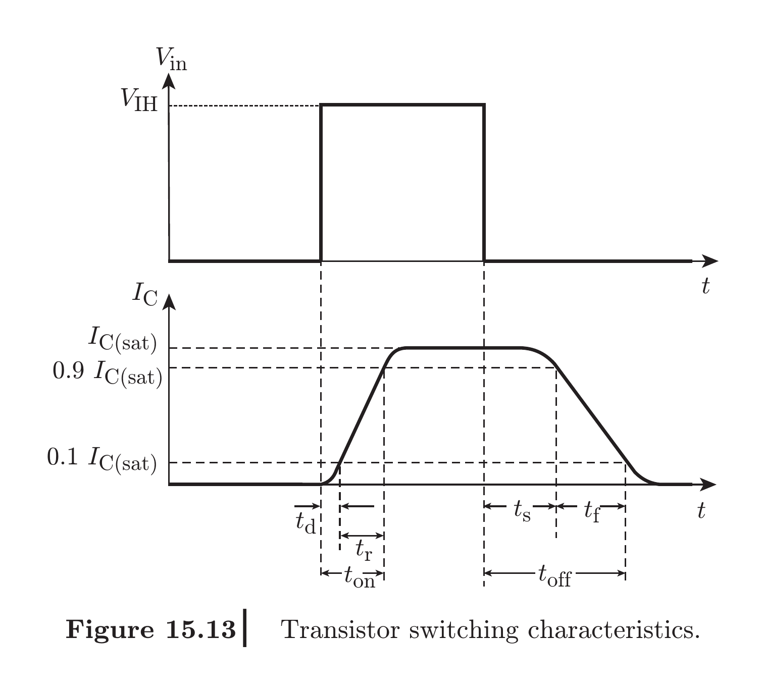
| Switching times | \(t_{ON}=t_d+t_r\); \(t_{OFF}=t_s+t_f\), often with \(t_s\) dominant | Turn-on/off depend on driver current and charge, approximately \(t\approx Q_g/I_g\); no storage-time interval |
| Conduction loss | \(P_{cond}\approx V_{CE(sat)}I_C\) | \(P_{cond}\approx I_{D,rms}^{2}R_{DS(on)}\) |
| Drive loss | Approximately \(P_B=V_{BE}I_B\) while ON | Approximately \(P_g=Q_gV_{GS}f_s\) |
| Temperature/paralleling | Current sharing is difficult; falling \(V_{BE}\) with temperature can promote thermal runaway | \(R_{DS(on)}\) normally rises with temperature, improving static current sharing |
| Integration/use | Lower density; useful where BJT gain or low saturation drop is advantageous | High density, fast switching and simple drive; dominant in CMOS/VLSI and high-frequency converters |
Switching operation. When a BJT is overdriven, both junctions become forward biased and excess base charge accumulates. Removing the input does not immediately stop collector current; reverse base drive or a Schottky clamp is used to shorten \(t_s\). A MOSFET stores no minority charge, but its gate is not lossless dynamically. The driver first raises \(V_{GS}\) to \(V_{th}\), then supplies the Miller charge while \(V_{DS}\) changes, and finally raises the gate to the full drive voltage. A low-impedance gate driver therefore reduces transition time and overlap loss.
For either device, an approximate hard-switching overlap loss is
where \(V\) is the blocked voltage (V), \(I\) the switched current (A), and \(f_s\) the switching frequency (Hz). Thus faster edges lower switching loss but increase \(dv/dt\), \(di/dt\) and electromagnetic interference.
Concise example: at \(I=10\,\text{A}\), a BJT with \(V_{CE(sat)}=0.2\,\text{V}\) dissipates \(2\,\text{W}\), while a MOSFET with \(R_{DS(on)}=20\,\text{m}\Omega\) also dissipates \(10^2(0.02)=2\,\text{W}\). Hence the MOSFET is not automatically lower-loss; current, voltage rating and temperature-dependent resistance matter. If that MOSFET has \(Q_g=40\,\text{nC}\), \(V_{GS}=10\,\text{V}\) and \(f_s=100\,\text{kHz}\), its gate-drive loss is only \(P_g=40\,\text{mW}\), but the driver must still supply the peak charge current.
Conclusion: MOSFETs are generally preferred for high-frequency, low-to-medium-voltage switching because they eliminate minority-carrier storage and need no continuous input current. BJTs remain useful where cost, gain or a nearly fixed saturation drop is favourable; device choice must compare total conduction, switching and drive losses at the actual operating point.
Practice target: 16–18 minutes; draw both switching mechanisms, reproduce the comparison table, and include the loss relations.