Computer Architecture
Possible Exam Questions
Exam Questions and Answer Map
[PYQ year] = observed in that past paper; [likely] = pattern-based prediction. Rehearse the answer plan closed-book, then use the links to check the complete answer in this chapter.
-
What is a system bus? Explain the different types of system bus (address, data, control). [1+4=5] — [PYQ 2079]
-
Answer plan: Define system bus → state its role (shared path among CPU, memory, I/O) → describe address bus (unidirectional, selects location) → data bus (bidirectional, transfers data) → control bus (carries read/write, interrupt, clock signals) → mention bus width impact.
-
Model answer: System Bus and Its Types
-
Explain the role of cache memory in a microcomputer; how does it improve performance over main memory? Illustrate with an example. [5] — [PYQ 2082]
-
Answer plan: Define cache → state locality of reference principle → explain hit/miss and hit ratio → give average access time formula \(T_{avg}=HT_c+(1-H)(T_c+T_m)\) → list mapping methods → numerical example.
-
Model answer: Cache Memory and Performance
-
Explain the memory hierarchy (registers, cache, main, virtual, auxiliary). [5–10] — [likely]
-
Answer plan: Draw/describe pyramid → list each level with volatility, speed, capacity, use → explain trade-off of speed vs cost vs size → relate to locality of reference.
-
Model answer: Computer Memory Hierarchy
-
Explain the basic organization of a CPU and the instruction cycle (fetch-decode-execute). [5–10] — [likely]
-
Answer plan: Draw CPU block (ALU, CU, registers) → list key registers (PC, IR, ACC, MAR, MDR) → describe each phase: fetch, decode, execute, write-back, update PC → mention addressing modes briefly.
-
Model answer: CPU Organization and Instruction Cycle
-
Explain virtual memory and the concept of paging. [5] — [likely]
-
Answer plan: Define virtual memory → explain page/frame/page-table mapping → describe page fault and its handling → mention thrashing → state advantages (larger-than-RAM programs, protection, multiprogramming).
-
Model answer: Virtual Memory and Paging
-
Explain cloud computing, its service/deployment types, and one application of each deployment type. [6] — [PYQ 2082]
-
Answer plan: Define on-demand shared resources → distinguish SaaS/PaaS/IaaS → distinguish public/private/hybrid deployment → give one real application for each deployment model.
- Model answer: Cloud Computing Models and Applications
Model Answer — System Bus and Its Types [1+4=5 marks, NTC 2079]
Exam-ready answer
(a) Definition [1 mark]
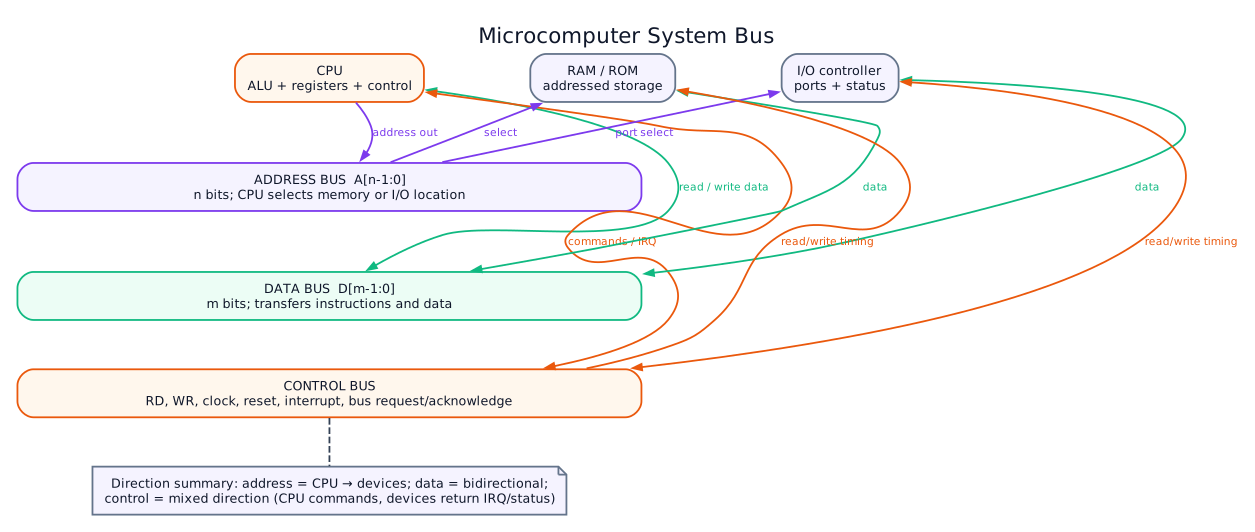
A system bus is the shared set of electrical signal paths that interconnects the CPU, main memory and I/O controllers so that they can exchange addresses, data and timing or command information. A complete transfer needs all three logical groups: the address identifies the source or destination, the control lines state the operation and timing, and the data lines carry the value.
(b) Types of system bus [4 marks]
| Bus | Normal direction | Information carried | Width or control significance |
|---|---|---|---|
| Address bus | Usually CPU → memory/I/O | Binary address of a memory location or I/O port | With \(n\) address lines, at most \(2^n\) distinct locations can be selected; byte-addressable capacity is \(2^n\) bytes. |
| Data bus | Bidirectional | Instructions, operands and results | An \(m\)-bit data bus transfers up to \(m\) bits per bus transaction; greater width raises transfer throughput but needs more pins and traces. |
| Control bus | Mixed direction | READ, WRITE, clock, reset, bus request/grant, interrupt request/acknowledge and ready/wait |
Establishes who controls the bus, the operation, synchronization and completion; it has no single source-to-destination direction. |
For a memory read, the CPU places an address on the address bus, asserts MEMORY READ, and waits for the selected memory to drive the data bus; a ready signal may end the cycle. For a write, the CPU places both address and data on their buses and asserts MEMORY WRITE. An interrupt travels from an I/O device toward the CPU, whereas an interrupt acknowledge travels back, illustrating why the control bus is mixed-direction.
Example: a byte-addressable processor with a 16-bit address bus can select
If its data bus is 8 bits wide, one byte moves per transaction; a 32-bit word requires four such transfers unless the interface supports a wider path. Bus width alone does not determine clock rate or total performance: arbitration delay, memory wait states, electrical loading and shared-bus contention can all reduce throughput. A fault on a shared address or control line may also affect every attached device, so systems use buffering, parity/error detection, access arbitration and timeouts where reliability is important.
Practice target: 8–9 minutes; allocate one mark to the definition, draw the labeled bus figure, and state direction, function and width effect for all three buses.
Model Answer — Cache Memory and Performance [5 marks, NTC 2082]
Exam-ready answer
Cache memory is a small, fast semiconductor memory placed logically between the CPU and main memory. It keeps copies of recently or frequently used instruction and data blocks so that most CPU references can be served without waiting for slower DRAM. Modern systems normally use a hierarchy such as private L1 instruction/data caches, larger L2 cache and a shared L3 cache.
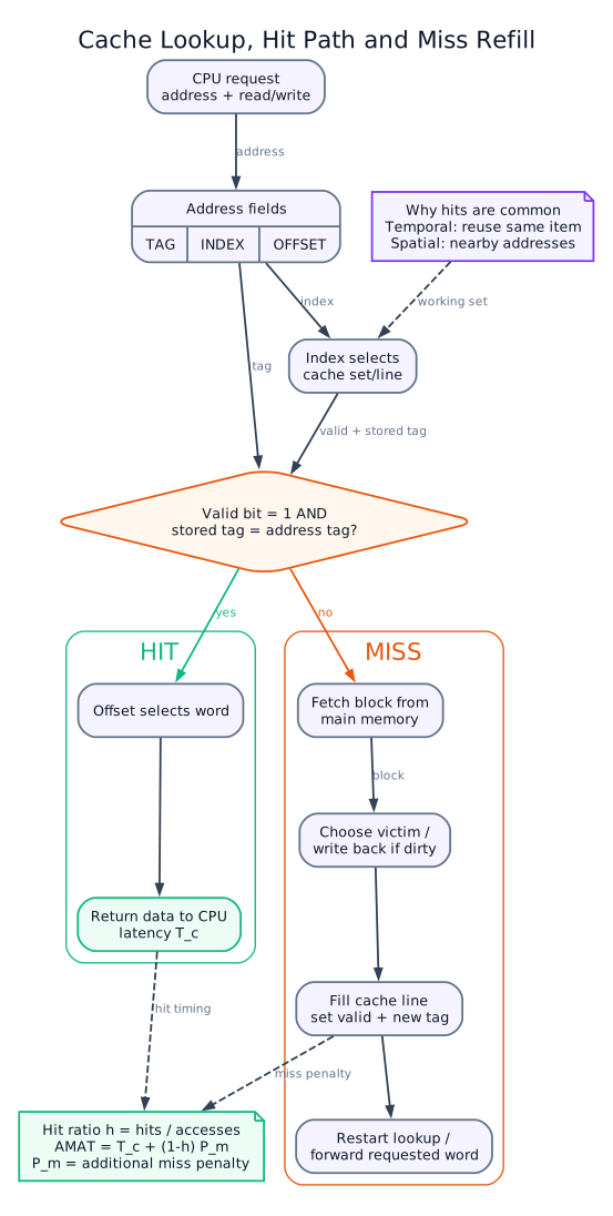
Its effectiveness follows locality of reference: temporal locality means a recently used item is likely to be reused, while spatial locality means nearby addresses are likely to be accessed soon. On a hit, the requested valid tag is found and data returns from cache. On a miss, a complete cache line is fetched from the next level, supplied to the CPU and installed for likely reuse.
| Mapping | Placement rule | Main trade-off |
|---|---|---|
| Direct mapped | One memory block has one possible cache line | Fast and cheap, but conflict misses are common |
| Fully associative | A block may occupy any line | Few placement conflicts, but expensive parallel tag search |
| Set associative | A block selects one set and any way in it | Practical balance of speed, cost and conflicts |
If \(H\) is hit ratio, \(T_c\) cache lookup time and \(T_m\) additional main-memory time on a miss, average memory access time is
Example: for \(H=0.95\), \(T_c=2\,\text{ns}\) and \(T_m=60\,\text{ns}\),
instead of about \(60\,\text{ns}\) for every uncached DRAM access, an idealized twelvefold reduction. Performance still falls for compulsory, capacity or conflict misses; writes require write-through or write-back policy, and multicore systems need cache coherence. Poor-locality workloads and cache side-channel leakage are limitations, so designers combine suitable line size/associativity with isolation and coherence controls.
Practice target: 8–9 minutes; define cache and both localities, explain hit/miss, write AMAT, and calculate the numerical example.
Model Answer — Computer Memory Hierarchy [5–10 marks]
5-mark answer and 10-mark extension
For 5 marks — write the memory-hierarchy core
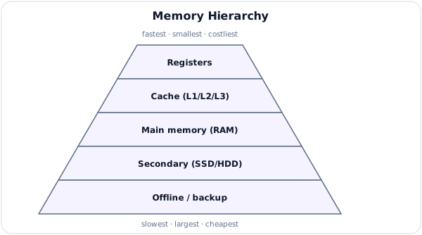
A memory hierarchy is the layered organization of storage by access time, capacity, cost per bit and proximity to the CPU. No single technology is simultaneously fastest, largest, cheapest and non-volatile, so frequently needed information is copied upward into small fast levels while bulk information remains in larger slow levels.
| Level | Typical property | Function |
|---|---|---|
| CPU registers | Fastest, few bytes/words, volatile | Hold current instruction, addresses, operands and results |
| Cache (L1/L2/L3) | Very fast SRAM, small, volatile | Holds recently used memory blocks |
| Main memory | DRAM, GB capacity, volatile | Holds active programs and data |
| Virtual memory | Address-space mechanism using RAM plus backing store | Maps process pages to frames and permits controlled overcommit |
| Auxiliary storage | SSD/HDD, large, non-volatile | Stores programs and files permanently |
Moving downward increases capacity and access time but decreases cost per bit; moving upward increases speed and cost per bit. Registers and cache are managed mainly by compiler/hardware, main and virtual memory by hardware plus the OS, and files by the OS and applications.
Add for a 10-mark variant — locality and AMAT
The hierarchy succeeds because programs exhibit temporal locality (recently referenced instructions/data tend to be reused), spatial locality (nearby addresses tend to be referenced) and sequential instruction access. Data moves between adjacent levels in blocks: cache lines between cache and RAM, pages between RAM and backing store, and file-system blocks between secondary storage and memory.
For one cache level, the average memory access time is
where \(T_{hit}\) is hit time, \(r_{miss}\) is miss rate and \(P_{miss}\) is the additional miss penalty. With \(T_{hit}=1\,\text{ns}\), miss rate \(=0.02\) and penalty \(=50\,\text{ns}\),
This illustrates why a small high-hit-ratio cache can make a large slow memory appear much faster. At the page level, a present page maps through the TLB/page table to a RAM frame; an absent valid page causes a page fault and disk/SSD service that is millions of CPU cycles slower. Virtual memory is therefore an address-management and protection facility, not a fast physical memory level.
| Comparison | Cache | Main memory | Auxiliary storage |
|---|---|---|---|
| Technology | SRAM | DRAM | Flash or magnetic media |
| CPU access | Hardware cache lookup | Direct through memory controller | Through I/O and OS |
| Unit moved | Cache line | Byte/word internally | Block/file |
| Persistence | No | No | Yes |
| Main limitation | Small, misses and coherence cost | Refresh and finite capacity | High latency and wear/mechanical delay |
The arrangement gives low average access time, economical capacity and process isolation, but it cannot remove all delays. Workloads larger than cache suffer capacity misses; random access defeats spatial locality; too few RAM frames cause page-fault thrashing; and sudden power loss destroys volatile levels. Error-correcting memory, access permissions, cache coherence, backups and replacement policies improve reliability and security but add hardware or software overhead.
Practice target: 9 minutes for the five-mark hierarchy or 17 minutes for the full answer; reproduce the pyramid, comparison and one AMAT calculation.
Model Answer — CPU Organization and Instruction Cycle [5–10 marks]
5-mark answer and 10-mark extension
For 5 marks — write the CPU-organization core
The central processing unit (CPU) is the programmable unit that fetches, decodes and executes machine instructions and coordinates memory and I/O. Its main parts are the ALU, which performs arithmetic, logic, shift and comparison operations; the control unit, which decodes instructions and issues timing/control signals; a high-speed register set; clocking; and internal address, data and control paths.
| Register | Purpose |
|---|---|
| PC | Address of the next instruction |
| IR | Current instruction being decoded/executed |
| MAR | Address presented for a memory access |
| MDR/MBR | Data or instruction word read from/written to memory |
| ACC/general registers | Operands and intermediate results |
| SP and flags | Stack top; zero, carry, sign and overflow status |
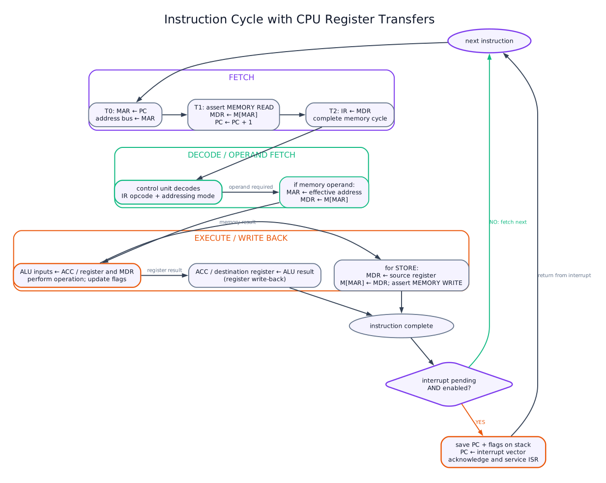
The basic cycle is: fetch the instruction addressed by PC into IR and advance PC; decode its opcode, operands and addressing mode; fetch operands if required; execute in the ALU, branch unit, memory or I/O unit; write back the result; then test pending interrupts before starting the next instruction.
Add for a 10-mark variant — register transfers and execution
For a fixed-length instruction, the fetch micro-operations may be written as
T0: MAR <- PC
T1: MDR <- Memory[MAR]; PC <- PC + instruction_length
T2: IR  <- MDR
T3: Decode IR.opcode, IR.mode and IR.operand fields
The control unit then calculates an effective address for direct, indirect, indexed or base-plus-offset addressing, requests the operand, selects the ALU operation, updates condition flags and enables the destination register or memory write. A typical logical instruction format is:
Example: for LOAD R1, [2000], decode identifies a memory-read operation and direct address 2000; the CPU performs MAR <- 2000, MDR <- Memory[MAR], then R1 <- MDR. For ADD R1, R2, both register values feed the ALU, the sum returns to R1, and zero/carry/overflow flags are updated. A branch replaces the sequential PC with its target only when its tested condition is true.
| Phase | Main control action | Possible delay/failure source |
|---|---|---|
| Fetch | Memory read using PC | Instruction-cache miss |
| Decode | Interpret fields and generate controls | Illegal opcode trap |
| Operand access | Read register or effective address | Data-cache/TLB miss, alignment fault |
| Execute | ALU, branch or I/O operation | Divide fault or branch penalty |
| Write-back | Enable destination and flags | Store-buffer or memory wait |
| Interrupt check | Save context and vector to handler | Disabled/masked request waits |
If an enabled interrupt is accepted, the CPU completes or precisely records the current instruction, saves PC and status, loads the handler address from an interrupt vector, services the event and restores context on return. Pipelined CPUs overlap stages of different instructions for throughput, but data, structural and control hazards can stall or flush the pipeline; this changes timing, not the logical fetch-decode-execute result. CPU performance is also limited by clock rate, memory latency, instruction-set design and available parallel execution units.
Practice target: 9 minutes for the five-mark core or 17–18 minutes for the full answer; include the register-transfer fetch sequence and one decoded instruction example.
Model Answer — Virtual Memory and Paging [5 marks]
Exam-ready answer
Virtual memory is a hardware-and-operating-system technique that gives each process a large, private logical address space independent of the amount and arrangement of physical RAM. In paging, virtual memory is divided into equal-size pages and RAM into same-size page frames. A virtual address has the bit format
The MMU first searches the translation lookaside buffer (TLB). On a TLB miss it reads the process page-table entry, whose essential fields include frame number, present/valid bit, read/write/execute protection, referenced bit and dirty bit. The physical address is formed without changing the offset:
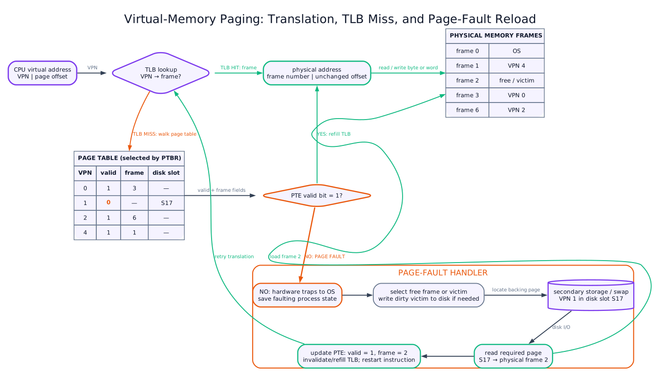
If a referenced, legal page is absent, a page fault traps to the OS. The OS validates the address, obtains a free frame or selects a victim, writes a dirty victim back if necessary, reads the required page from secondary storage, updates the page table/TLB and restarts the faulting instruction. An illegal address or forbidden access instead terminates/signals the process; it is not demand-paged in.
Example: with 16-bit virtual addresses and \(4\,\text{KiB}=2^{12}\)-byte pages, the offset is 12 bits and the VPN is 4 bits. Address 0x3ABC is VPN 0x3, offset 0xABC; if page 3 maps to frame 9, the physical address is 0x9ABC.
Paging lets programs exceed RAM, supports relocation, multiprogramming, shared pages and per-page protection. Its costs are page-table storage, translation overhead, internal fragmentation and very slow faults. If active working sets exceed RAM, repeated replacement causes thrashing; sufficient frames, locality-aware replacement and working-set control are therefore essential.
Practice target: 8–9 minutes; draw the paging path, preserve the offset in the address example, and list every page-fault handling step in order.
Model Answer — Cloud Computing Models and Applications [6 marks, NTC 2082]
Exam-ready answer
Cloud computing is the on-demand delivery over a network of a shared pool of configurable computing resources such as servers, storage, platforms and applications. Resources can be rapidly provisioned and released with minimal provider interaction, are pooled among users, scale elastically and are measured for billing or control.
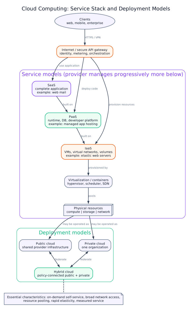
| Service model | Provider manages / customer receives | Customer mainly manages | Example use |
|---|---|---|---|
| SaaS | Complete hosted application through browser/API | Users, data and configuration | Web mail or an online office suite |
| PaaS | Infrastructure, OS, runtime, middleware and managed database | Application code and data | Deploying a telecom self-care web API without administering servers |
| IaaS | Virtual machines, virtual network and storage | Guest OS, middleware, applications and data | Creating elastic web-server VMs and block storage |
| Deployment | Ownership/access | One suitable application |
|---|---|---|
| Public cloud | Provider-owned, logically shared by many tenants over public/private links | A startup hosts a public website whose capacity scales during demand peaks |
| Private cloud | Dedicated to one organization on-premises or hosted | A telecom operator runs subscriber and billing systems under internal policy |
| Hybrid cloud | Policy-connected private and public clouds with workload/data movement | Customer records remain private while public cloud supplies burst computing or encrypted backup |
A typical request is authenticated at the portal/API, scheduled onto pooled virtualized or containerized resources, connected to storage/network services, monitored, scaled and metered. Benefits are rapid deployment, elasticity, broad access, resource sharing and reduced initial capital expense. Limitations include provider dependence, latency/outage risk, migration lock-in, unpredictable recurring cost and legal data-location requirements. Controls should include strong IAM and MFA, least privilege, encryption in transit/at rest, tenant isolation, logs, backups, key management and a clear shared-responsibility agreement; moving to cloud does not transfer all security responsibility to the provider.
Practice target: 10–11 minutes; define the essential characteristics, reproduce both three-row matrices, and give one application for every deployment model.
Syllabus Focus
- I/O devices and storage devices
- Main, auxiliary, virtual, and cache memory
- CPU and memory organization
- System buses
- Microprocessor fundamentals
1. Computer System Overview
Likely Exam Question (5 marks)
"Draw the block diagram of a computer system and explain the functions of its major units."
A computer is an electronic programmable machine that accepts data as input, processes it according to stored instructions, stores data/results, and produces output.
Basic Block Diagram
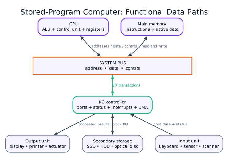
Major Functional Units
| Unit | Function | Examples |
|---|---|---|
| Input unit | Accepts data and instructions | Keyboard, mouse, scanner, microphone |
| Output unit | Presents processed information | Monitor, printer, speaker |
| Memory unit | Stores instructions and data | RAM, ROM, cache |
| ALU | Performs arithmetic and logical operations | Addition, comparison, AND/OR |
| Control unit | Coordinates all operations | Fetch, decode, control signals |
| Secondary storage | Stores data permanently | SSD, HDD, optical disk, magnetic tape |
The modern computer is based on the stored-program concept, where instructions and data are stored in the same memory and fetched by the CPU during execution.
2. Input and Output Devices
Input Devices
Input devices convert user actions or physical signals into digital data that can be processed by the computer.
| Device | Use |
|---|---|
| Keyboard | Text and command input |
| Mouse/touchpad | Pointer control |
| Scanner | Converts printed text/images into digital form |
| Microphone | Audio input |
| Camera/webcam | Image and video input |
| Barcode/QR reader | Product and identity code scanning |
| Sensors | Physical measurement such as temperature, pressure, light |
Output Devices
Output devices convert digital results into human-readable or machine-usable form.
| Device | Use |
|---|---|
| Monitor | Visual output |
| Printer | Hard-copy output |
| Speaker | Audio output |
| Plotter | Large engineering drawings/maps |
| Actuator | Physical control in automation systems |
I/O Interfaces
An I/O interface connects peripheral devices to the CPU and memory system. It handles speed matching, data format conversion, control signals, and status reporting.
Common I/O methods:
| Method | Description | Advantage | Disadvantage |
|---|---|---|---|
| Programmed I/O | CPU repeatedly checks device status | Simple | Wastes CPU time |
| Interrupt-driven I/O | Device interrupts CPU when ready | Better CPU utilization | Interrupt overhead |
| DMA | Direct Memory Access controller transfers blocks between I/O and memory | Fast for large data transfer | Needs extra hardware/control |
3. Memory and Storage Systems
Likely Exam Question (10 marks)
"Explain the memory hierarchy of a computer system. Compare cache, main memory, and secondary storage."
Computer memory is organized as a hierarchy to balance speed, cost, and capacity.
Memory Hierarchy
| Level | Volatile? | Speed | Capacity | Main Use |
|---|---|---|---|---|
| Registers | Yes | Fastest | Very small | Current operands/instructions |
| Cache | Yes | Very fast | Small | Frequently used data/instructions |
| Main memory | Yes | Medium | GB range | Running programs and data |
| Secondary storage | No | Slower | GB/TB range | Permanent storage |
| Backup storage | No | Slowest | Very large | Archival and recovery |
Main Memory
Main memory is directly accessible by the CPU. It stores currently executing programs and active data.
Main types:
- RAM (Random Access Memory): volatile read/write memory.
- ROM (Read Only Memory): non-volatile memory used for firmware/boot code.
RAM types:
| Type | Feature | Use |
|---|---|---|
| SRAM | Fast, no refresh, costly, low density | Cache memory |
| DRAM | Slower, needs refresh, cheap, high density | Main memory |
ROM types:
| Type | Feature |
|---|---|
| PROM | Programmable once |
| EPROM | Erased by UV light |
| EEPROM | Electrically erasable, byte-level |
| Flash | Electrically erasable, block-level |
Auxiliary / Secondary Storage
Auxiliary storage is non-volatile storage used for permanent data and program storage.
| Storage | Characteristics | Examples/Use |
|---|---|---|
| HDD | Magnetic disk, mechanical moving parts, low cost per GB | Bulk storage |
| SSD | Flash-based, no moving parts, fast access | OS and application storage |
| Optical disk | Laser-based read/write | CD, DVD, Blu-ray |
| Magnetic tape | Sequential access, very high capacity | Backup/archive |
Cache Memory
Cache memory is a small, high-speed memory placed between CPU and main memory. It stores copies of frequently used data/instructions to reduce average memory access time.
Key terms:
- Cache hit: requested data is found in cache.
- Cache miss: requested data is not in cache and must be fetched from main memory.
- Hit ratio: fraction of memory accesses served by cache.
- Miss ratio: \(1 - \text{hit ratio}\).
Average memory access time:
where \(H\) is hit ratio, \(T_c\) is cache access time, and \(T_m\) is main-memory access time after a miss.
Cache mapping methods:
| Method | Idea | Feature |
|---|---|---|
| Direct mapping | Each memory block maps to one cache line | Simple, but more conflicts |
| Fully associative | A block may go anywhere in cache | Flexible, costly hardware |
| Set associative | Block maps to a set, then any line in that set | Balance of cost and performance |
Virtual Memory
Virtual memory gives a program the illusion of a large continuous memory space even when physical RAM is limited. It uses secondary storage as an extension of main memory.
Important terms:
- Page: fixed-size block of virtual memory.
- Frame: fixed-size block of physical memory.
- Page table: maps virtual pages to physical frames.
- Page fault: occurs when required page is not in RAM and must be loaded from disk.
- Thrashing: excessive page faults causing very poor performance.
Advantages of virtual memory:
- Allows programs larger than physical RAM.
- Provides memory protection between processes.
- Improves multiprogramming.
- Simplifies program loading and relocation.
4. CPU Organization
Likely Exam Question (10 marks)
"Explain the organization of CPU with ALU, control unit, and registers. Describe the instruction cycle."
The Central Processing Unit (CPU) executes program instructions and controls the operation of the computer.
CPU Components
| Component | Function |
|---|---|
| ALU | Performs arithmetic and logical operations |
| Control unit | Fetches, decodes, and controls instruction execution |
| Registers | Very fast temporary storage inside CPU |
| Clock | Synchronizes CPU operations |
| Internal bus | Transfers data inside CPU |
Important CPU Registers
| Register | Full Name | Function |
|---|---|---|
| PC | Program Counter | Address of next instruction |
| IR | Instruction Register | Current instruction being decoded/executed |
| ACC | Accumulator | Intermediate arithmetic/logic result |
| MAR | Memory Address Register | Address of memory location to access |
| MDR/MBR | Memory Data/Buffer Register | Data read from or written to memory |
| SP | Stack Pointer | Address of top of stack |
| Flag register | Status register | Carry, zero, sign, overflow, parity flags |
Instruction Cycle
- Fetch: CPU uses PC to read instruction from memory into IR.
- Decode: Control unit interprets opcode and addressing mode.
- Execute: ALU/I/O/memory operation is performed.
- Write back: Result is stored in register or memory.
- Update PC: PC points to next instruction or branch target.
Instruction Format
An instruction generally contains:
- Opcode: operation to be performed, such as ADD, LOAD, STORE, JUMP.
- Operand: data or address of data.
- Addressing mode: method used to locate operand.
Common addressing modes:
| Mode | Meaning | Example idea |
|---|---|---|
| Immediate | Operand is part of instruction | MOV A, #05H |
| Register | Operand is in register | ADD A, B |
| Direct | Address is given in instruction | Load from memory address 2050H |
| Indirect | Instruction points to address holder | Address stored in register/memory |
| Indexed | Effective address = base + index | Array access |
5. Bus Organization
Likely Exam Question (5 marks)
"Differentiate between address bus, data bus, and control bus."
A bus is a shared communication path that transfers data, addresses, and control signals among CPU, memory, and I/O devices.
Types of System Bus
| Bus | Direction | Function |
|---|---|---|
| Address bus | Mostly CPU to memory/I/O | Selects memory location or I/O port |
| Data bus | Bidirectional | Transfers actual data/instructions |
| Control bus | Both directions | Carries read/write, interrupt, clock, reset signals |
Bus Width
- If address bus has \(n\) lines, maximum addressable locations = \(2^n\).
- If data bus has \(m\) lines, CPU can transfer \(m\) bits at a time.
Example: A 16-bit address bus can address:
Bus Types
| Type | Description |
|---|---|
| Internal bus | Connects units inside CPU |
| System bus | Connects CPU, memory, and I/O controller |
| Expansion bus | Connects external/peripheral devices |
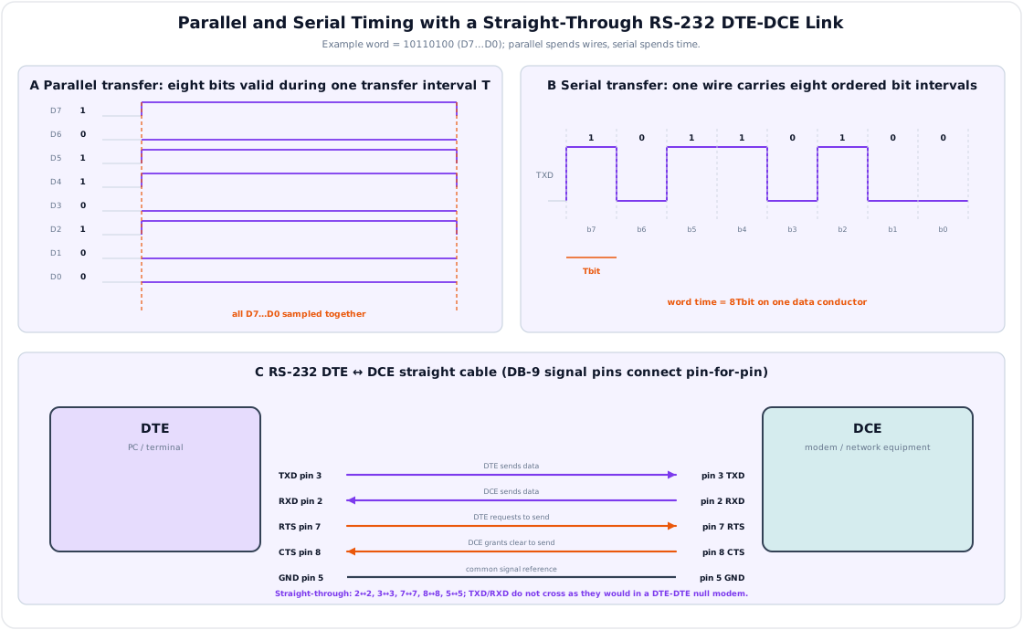
| Parallel bus | Multiple bits transmitted simultaneously |
| Serial bus | Bits transmitted one after another |
Examples: PCIe, USB, SATA, I2C, SPI, memory bus.
6. Microprocessor Fundamentals
Likely Exam Question (10 marks)
"Define microprocessor. Explain its main characteristics and basic working."
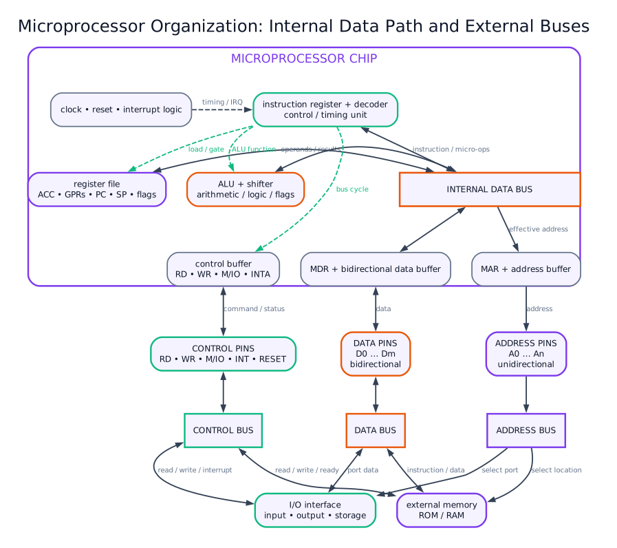
A microprocessor is a programmable VLSI/ULSI chip that contains the CPU functions of a computer: ALU, control unit, registers, and instruction execution logic.
It is the brain of a microcomputer, but it requires external memory, I/O devices, clock, and power supply to form a complete system.
Microprocessor-Based System
Main Characteristics
| Characteristic | Meaning |
|---|---|
| Word length | Number of bits processed at a time, such as 8/16/32/64-bit |
| Clock speed | Number of clock cycles per second |
| Instruction set | Operations the processor can execute |
| Address bus width | Maximum memory that can be addressed |
| Data bus width | Number of data bits transferred at once |
| Register set | Internal storage available to CPU |
RISC vs CISC
| Feature | RISC | CISC |
|---|---|---|
| Full form | Reduced Instruction Set Computer | Complex Instruction Set Computer |
| Instruction count | Fewer, simpler instructions | Many complex instructions |
| Execution | Usually one/few cycles | May take many cycles |
| Hardware | Simpler control | More complex control |
| Examples | ARM, RISC-V | x86 |
Microprocessor vs Microcontroller
| Feature | Microprocessor | Microcontroller |
|---|---|---|
| Integration | CPU mainly | CPU + memory + I/O on one chip |
| External components | More required | Fewer required |
| Application | PCs, servers, high-performance systems | Embedded control systems |
| Cost/power | Higher | Lower |
7. Cloud Computing
Cloud computing delivers a shared pool of compute, storage, network and application resources over a network on demand, with rapid elasticity and measured use.
| Service model | Customer receives | Example |
|---|---|---|
| SaaS | Complete hosted application | Web mail or online office suite |
| PaaS | Managed runtime, database and developer platform | Deploying a web API without managing servers |
| IaaS | Virtual machines, networks and block/object storage | Elastic web-server infrastructure |
| Deployment model | Ownership/access | Real application |
|---|---|---|
| Public cloud | Shared provider infrastructure for many customers | Startup hosts a public website and scales on demand |
| Private cloud | Dedicated to one organization | Telecom operator hosts subscriber and billing systems under internal control |
| Hybrid cloud | Policy-connected public and private resources | Private customer database with public-cloud burst capacity or backup |
8. Quick Comparisons
RAM vs ROM
| Feature | RAM | ROM |
|---|---|---|
| Volatility | Volatile | Non-volatile |
| Operation | Read/write | Mostly read |
| Use | Running programs/data | Firmware/boot program |
| Speed | Faster | Usually slower |
Cache vs Virtual Memory
| Feature | Cache Memory | Virtual Memory |
|---|---|---|
| Purpose | Speeds up CPU-memory access | Extends apparent main memory |
| Managed by | Hardware mostly | OS + hardware MMU |
| Located between | CPU and RAM | RAM and secondary storage |
| Unit | Cache line/block | Page/frame |
Primary vs Secondary Memory
| Feature | Primary Memory | Secondary Memory |
|---|---|---|
| CPU access | Direct | Indirect via I/O/storage controller |
| Volatility | Mostly volatile | Non-volatile |
| Speed | Faster | Slower |
| Capacity | Smaller | Larger |
Key Exam Points - Computer Architecture
- CPU consists of ALU, control unit, and registers.
- Main memory is directly accessible by CPU; secondary storage is permanent but slower.
- Cache reduces average memory access time using locality of reference.
- Virtual memory uses paging and page tables; page fault occurs when a page is absent from RAM.
- Address bus width determines maximum addressable memory: \(2^n\) locations for \(n\) address lines.
- A microprocessor is CPU on a chip; a microcontroller includes CPU, memory, and I/O on one chip.