Optical Components
Possible Exam Questions
Exam Questions and Answer Map
These are pattern-based predictions, not claimed past questions. For each one, rehearse the answer plan closed-book, then use the links to check the complete answer in this chapter.
-
Draw the block diagram of a fiber-optic communication system and explain each component. [5–10] — [likely]
-
Answer plan: Draw full block diagram (source → encoder/driver → optical source → fiber → photodetector → amplifier/decision → output) → explain function of each block → name component examples (LED/LD, PIN/APD) → mention connectors and test equipment.
-
Model answer: Fiber-Optic Communication System and Components
-
Compare LED and laser diode as optical sources. [5] — [likely]
-
Answer plan: State emission process (spontaneous vs stimulated) → compare coherence, spectral width, output power, modulation speed, cost, temperature sensitivity → state fiber suitability (LED for short MMF, LD for long SMF) → draw comparison table.
-
Model answer: LED and Laser Diode as Optical Sources
-
Explain PIN and avalanche (APD) photodetectors and compare them. [5–10] — [likely]
-
Answer plan: Define photodetection → explain PIN structure (P-I-N layers, reverse bias, no gain) → explain APD (high field, impact ionization, internal gain) → compare sensitivity, bias voltage, noise, cost, and application → write responsivity formula \(R = I_p/P_{opt}\).
-
Model answer: PIN and Avalanche Photodiodes
-
What are the main differences between optical transmitters and optical receivers? [2–5] — [PYQ 2081]
-
Answer plan: Define transmitter (electrical→optical, LED/LD, driver circuit) → define receiver (optical→electrical, PIN/APD, amplifier, decision circuit) → compare function, key component, signal direction, and performance metrics.
-
Model answer: Optical Transmitter and Receiver Differences
-
Explain fiber connectors, splicing techniques and the working of an OTDR. [5–10] — [likely]
-
Answer plan: Define connectors → list common types (SC, LC, ST, FC) → list loss sources → define splicing (fusion vs mechanical) with comparison table → explain OTDR principle (backscatter + Fresnel reflection, \(d = vt/2\)) → sketch OTDR trace showing events.
- Model answer: Fiber Connectors, Splicing and OTDR Testing
Scope of this Chapter
This chapter covers the Optical Components part of NTC Paper II, Section B, Topic 7: LED, laser diode, photodetectors, PIN, APD, connectors, splicing, and OTDR.
1. Optical Fiber Communication System Components
Likely Exam Question (5 marks)
"Draw and explain the block diagram of an optical fiber communication system."
Basic Block Diagram

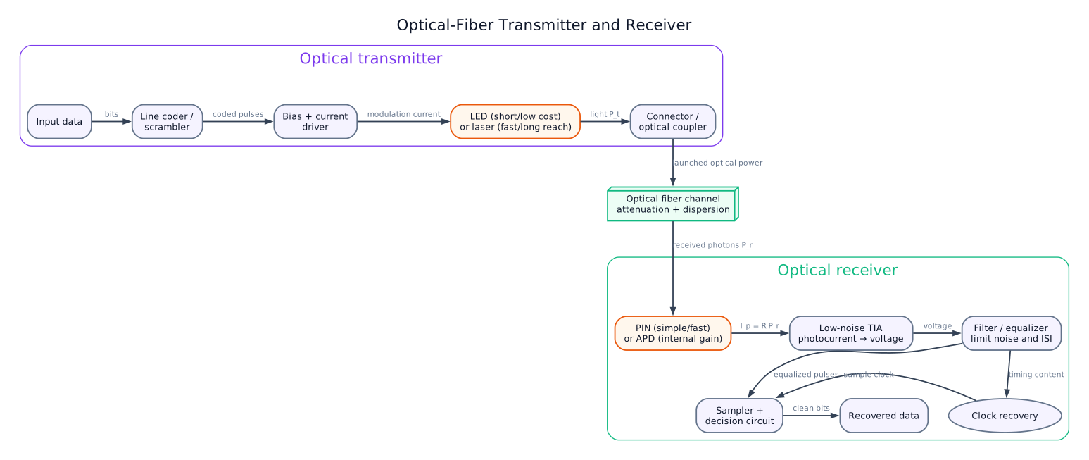
Main Components
| Component | Function |
|---|---|
| Optical source | Converts electrical signal to optical signal |
| Optical fiber | Guides light from transmitter to receiver |
| Connectors/splices | Join fibers or connect equipment |
| Photodetector | Converts optical signal to electrical signal |
| Receiver amplifier | Amplifies weak photocurrent |
| OTDR/test equipment | Tests length, loss, splice quality, and faults |
2. Optical Sources
Likely Exam Question (10 marks)
"Compare LED and laser diode as optical sources used in fiber communication."
An optical source converts input electrical current into light.
The two main optical sources are:
- Light Emitting Diode (LED)
- Laser Diode (LD)
Important requirements of an optical source:
- Emission wavelength should match low-loss fiber windows.
- Output optical power should be sufficient.
- Spectral width should be narrow for high-speed systems.
- Coupling efficiency into the fiber should be high.
- Response speed should support required bit rate.
- Source should be reliable, compact, and efficient.
3. Light Emitting Diode (LED)
Likely Exam Question (5 marks)
"Explain LED as an optical source. Mention its advantages and limitations."
Definition
An LED is a semiconductor p-n junction device that emits light due to spontaneous emission when forward biased.
When electrons and holes recombine in the active region, energy is released as photons.
Features
| Feature | LED |
|---|---|
| Emission process | Spontaneous emission |
| Output light | Incoherent |
| Spectral width | Wide |
| Output power | Low to moderate |
| Modulation speed | Lower than laser diode |
| Cost | Low |
| Fiber coupling | Better with multimode fiber |
Advantages
- Simple construction.
- Low cost.
- Long life and high reliability.
- Less temperature sensitive than laser diode.
- Suitable for short-distance multimode fiber links.
Limitations
- Low optical output power.
- Wide spectral width causes chromatic dispersion.
- Lower modulation bandwidth.
- Poor coupling into single-mode fiber.
LED Types
| Type | Description |
|---|---|
| Surface-emitting LED | Emits light perpendicular to junction plane; simple but low coupling efficiency |
| Edge-emitting LED | Emits light from edge; narrower beam and better coupling |
4. Laser Diode
Likely Exam Question (10 marks)
"Explain the working of a laser diode and compare it with an LED."
Definition
A laser diode is a semiconductor optical source that emits coherent light by stimulated emission.
LASER means Light Amplification by Stimulated Emission of Radiation.
Working Principle
When the laser diode is forward biased, carrier injection occurs in the active region.
If injection current exceeds the threshold current, stimulated emission dominates and intense coherent light is produced.
The cleaved semiconductor faces act as mirrors and form an optical resonant cavity.
Important Terms
| Term | Meaning |
|---|---|
| Spontaneous emission | Random photon emission without external triggering |
| Stimulated emission | Incident photon causes emission of another identical photon |
| Population inversion | More electrons in excited state than lower state |
| Threshold current | Minimum current at which lasing action begins |
| Coherent light | Light waves have fixed phase relationship |
| Monochromatic light | Very narrow spectral width |
Characteristics
| Feature | Laser Diode |
|---|---|
| Emission process | Stimulated emission |
| Output light | Coherent and directional |
| Spectral width | Narrow |
| Output power | High |
| Modulation speed | Very high |
| Coupling | Excellent with single-mode fiber |
| Temperature effect | More sensitive |
Advantages
- High optical output power.
- Narrow spectral width reduces chromatic dispersion.
- High modulation bandwidth.
- Efficient coupling into single-mode fiber.
- Suitable for long-distance and high-bit-rate links.
Limitations
- Higher cost.
- Requires temperature control and stable biasing.
- Has threshold current.
- Shorter lifetime than LED if improperly driven.
- Eye safety precautions are required.
LED vs Laser Diode
| Feature | LED | Laser Diode |
|---|---|---|
| Emission | Spontaneous | Stimulated |
| Light | Incoherent | Coherent |
| Spectrum | Broad | Narrow |
| Beam divergence | Wide | Narrow |
| Output power | Low | High |
| Speed | Low to moderate | High |
| Cost | Low | High |
| Temperature sensitivity | Low | High |
| Best suited for | Short MMF links | Long SMF links |
5. Photodetectors
Likely Exam Question (5 marks)
"What is a photodetector? State the requirements of photodetectors used in optical receivers."
Definition
A photodetector converts received optical power into electrical current.
The photocurrent is proportional to the incident optical power.
Requirements
- High sensitivity at operating wavelength.
- Fast response time.
- Low noise and low dark current.
- High quantum efficiency.
- Small size and compatibility with fiber coupling.
- Reliable operation and stable characteristics.
Important Parameters
| Parameter | Meaning |
|---|---|
| Responsivity | Photocurrent produced per watt of optical power |
| Quantum efficiency | Fraction of incident photons that generate electron-hole pairs |
| Dark current | Current flowing without incident light |
| Response time | Speed of detector response |
| Noise equivalent power | Minimum detectable optical power related to noise |
Responsivity
where:
- \(R\) = responsivity in A/W
- \(I_p\) = photocurrent
- \(P_{opt}\) = incident optical power
Responsivity in terms of quantum efficiency:
or:
where:
- \(\eta\) = quantum efficiency
- \(q\) = electron charge
- \(h\) = Planck's constant
- \(f\) = optical frequency
- \(\lambda\) = wavelength
6. PIN Photodiode
Likely Exam Question (5 marks)
"Explain the construction and working of a PIN photodiode."
Definition
A PIN photodiode is a photodetector with p-type, intrinsic, and n-type semiconductor layers.
It is reverse biased during operation.
Construction
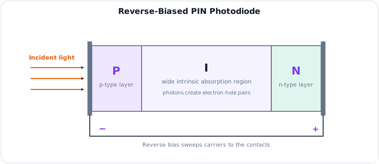
The intrinsic region is wide, so most photons are absorbed there and create electron-hole pairs.
Working
- Incident photons enter the intrinsic region.
- Photons with sufficient energy create electron-hole pairs.
- Reverse-bias electric field sweeps carriers quickly to terminals.
- A photocurrent proportional to optical power is produced.
Advantages
- Low noise.
- Simple biasing.
- Good linearity.
- Fast response.
- Suitable for many digital fiber receivers.
Limitations
- No internal gain.
- Less sensitive than APD for very weak optical signals.
7. Avalanche Photodiode (APD)
Likely Exam Question (10 marks)
"What is an avalanche photodiode? Compare PIN photodiode and APD."
Definition
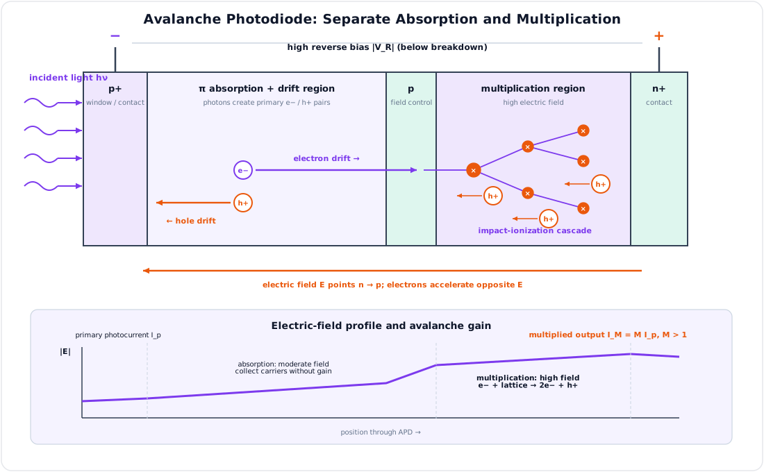
An avalanche photodiode (APD) is a reverse-biased photodiode operated at high electric field so that carriers gain enough energy to create additional carriers by impact ionization.
This gives internal current gain.
Working
- Incident light generates primary electron-hole pairs.
- High reverse field accelerates carriers.
- Accelerated carriers collide with atoms and create more electron-hole pairs.
- Avalanche multiplication increases photocurrent.
Advantages
- Higher sensitivity than PIN photodiode.
- Internal gain improves receiver performance.
- Useful for long-distance links with weak received power.
Limitations
- Requires high reverse bias.
- More noise due to avalanche multiplication.
- Temperature sensitive.
- More expensive and complex bias control.
PIN vs APD
| Feature | PIN Photodiode | APD |
|---|---|---|
| Internal gain | No | Yes |
| Sensitivity | Moderate | High |
| Bias voltage | Low | High |
| Noise | Low | Higher |
| Cost | Lower | Higher |
| Circuit complexity | Simple | Complex |
| Temperature sensitivity | Lower | Higher |
| Typical use | Short/medium links | Long links, weak signals |
8. Optical Connectors
Likely Exam Question (5 marks)
"What are optical fiber connectors? Mention common connector types and sources of connector loss."
Definition
An optical connector is a detachable device used to connect optical fibers to equipment, patch panels, or other fibers.
Requirements of a Good Connector
- Low insertion loss.
- Low return loss.
- Repeatable connection performance.
- Good mechanical strength.
- Easy installation and maintenance.
- Stable performance under temperature and vibration.
Common Connector Types
| Connector | Feature | Common Use |
|---|---|---|
| SC | Push-pull square connector | Telecom, FTTH |
| LC | Small form-factor latch connector | High-density patch panels, SFPs |
| ST | Bayonet twist connector | Older LAN systems |
| FC | Threaded connector | Test equipment, high-vibration areas |
| MPO/MTP | Multi-fiber connector | Data centers, ribbon fiber |
Connector Losses
| Loss Source | Explanation |
|---|---|
| Lateral misalignment | Fiber cores do not face each other exactly |
| Angular misalignment | Fiber axes meet at an angle |
| End separation | Air gap between fiber ends |
| End-face defect | Scratch, dirt, or poor polishing |
| Core diameter mismatch | Different fiber types connected |
| Fresnel reflection | Reflection at glass-air interface |
Insertion Loss and Return Loss
Insertion loss is the power loss caused by inserting a connector or component:
Return loss measures reflected power:
Higher return loss means lower reflection and better connection quality.
9. Fiber Splicing
Likely Exam Question (10 marks)
"Explain fusion splicing and mechanical splicing of optical fiber. Compare them."
Definition
Splicing is the permanent joining of two optical fibers.
Splicing is used in cable installation, repair, route extension, and fiber distribution networks.
Types of Splicing
- Fusion splicing
- Mechanical splicing
Fusion Splicing
In fusion splicing, two fiber ends are aligned and melted together using an electric arc.
Steps:
- Strip protective coating.
- Clean the fiber.
- Cleave fiber ends accurately.
- Align fibers in fusion splicer.
- Fuse using electric arc.
- Protect splice using heat-shrink sleeve.
- Test splice loss.
Advantages:
- Very low splice loss.
- High mechanical strength.
- Low reflection.
- Best for long-distance and permanent links.
Limitations:
- Splicing machine is expensive.
- Requires power and trained operator.
Mechanical Splicing
In mechanical splicing, two cleaved fiber ends are aligned inside a mechanical holder using index-matching gel.
Advantages:
- Quick and simple.
- No fusion splicer required.
- Useful for temporary restoration.
Limitations:
- Higher loss than fusion splice.
- Higher reflection.
- Lower long-term reliability.
Fusion vs Mechanical Splicing
| Feature | Fusion Splice | Mechanical Splice |
|---|---|---|
| Joint type | Permanent fused glass | Mechanical alignment |
| Typical loss | Very low | Higher |
| Reflection | Very low | Higher |
| Equipment cost | High | Low |
| Skill | Requires trained operator | Easier |
| Reliability | High | Moderate |
| Use | Long-haul, FTTH, permanent repair | Temporary repair, quick restoration |
10. OTDR
Likely Exam Question (10 marks)
"What is OTDR? Explain its working and uses in optical fiber testing."
Definition
An Optical Time Domain Reflectometer (OTDR) is an optical test instrument used to locate faults, measure fiber length, estimate attenuation, and identify splice or connector losses.
Working Principle
OTDR works on the principle of Rayleigh backscattering and Fresnel reflection.
It sends a short optical pulse into the fiber and measures the returned light as a function of time.
Because light velocity in fiber is known, the distance to a fault or event can be calculated:
where:
- \(d\) = distance to event
- \(v = c/n\) = velocity of light in fiber
- \(t\) = round-trip time
- Factor 2 is used because the pulse travels to the event and back
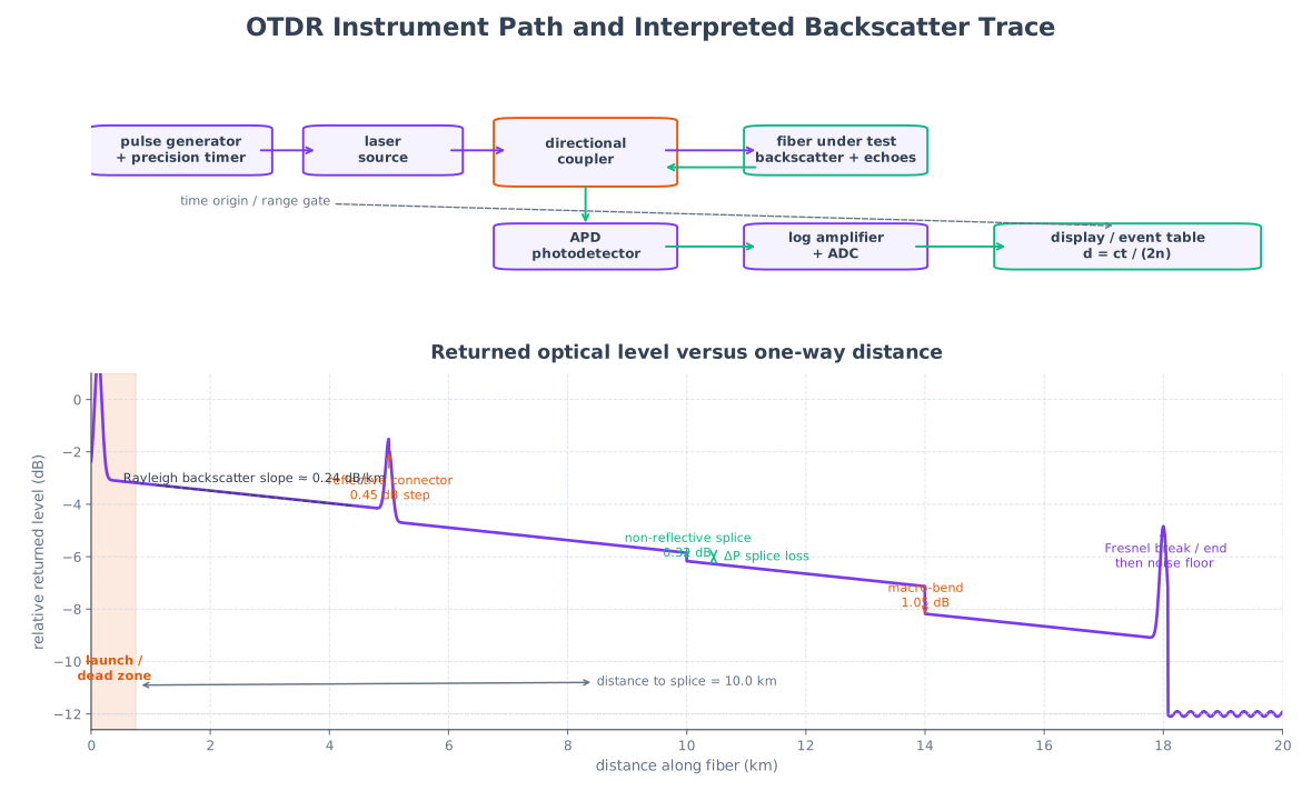
OTDR Trace Events
| Event | Appearance | Cause |
|---|---|---|
| Fiber attenuation | Gradual downward slope | Distributed loss |
| Connector | Reflection spike and loss step | Fresnel reflection |
| Fusion splice | Small loss step, usually no reflection | Permanent splice |
| Bend loss | Sudden loss step | Tight bend or stress |
| Fiber break | Large reflection or end spike | Open fiber end |
Uses of OTDR
- Measure fiber length.
- Locate fiber break or fault.
- Measure splice and connector loss.
- Estimate fiber attenuation in dB/km.
- Create acceptance-test records after installation.
- Troubleshoot FTTH and backbone links.
Important OTDR Settings
| Setting | Effect |
|---|---|
| Wavelength | Test at 1310 or 1550 nm depending on link requirement |
| Pulse width | Longer pulse gives longer range but poorer resolution |
| Range | Maximum fiber distance shown |
| Averaging time | Longer averaging improves trace clarity |
| Refractive index | Needed for accurate distance measurement |
Dead Zone
Dead zone is the distance after a strong reflection where the OTDR cannot accurately detect another nearby event.
Dead zones are reduced by using proper pulse width and launch fiber.
Model Answer — Fiber-Optic Communication System and Components [5–10 marks]
5-mark answer and 10-mark extension
For 5 marks — core system chain
A fiber-optic communication system carries an information-bearing electrical signal by converting it to light, guiding that light through a dielectric fiber and converting it back to an electrical signal. Its physical path is
- Input/encoder: formats voice, video or data and may add line coding.
- Source driver and optical source: the driver modulates an LED for economical short multimode links or a laser diode for high-speed single-mode links.
- Coupler, connectors and splices: launch light into the core and join cable sections while adding small insertion losses.
- Optical fiber channel: core and lower-index cladding guide light by total internal reflection; attenuation reduces power and dispersion broadens pulses.
- Photodetector: a reverse-biased PIN or APD converts received optical power to photocurrent, \(I_p=RP_r\), where \(R\) is in A/W and \(P_r\) in W.
- Receiver: a transimpedance amplifier, filter/equalizer, clock recovery and decision circuit reconstruct the output bits.
The basic power test is
with every subtracted term in dB; \(P_r\) must exceed receiver sensitivity. The system provides huge bandwidth, low loss, EMI immunity and electrical isolation, but needs careful source/fiber matching, precise joints and electro-optic equipment.
Add for a 10-mark system explanation
At the transmitter, the line coder produces a timing-suitable waveform, the current driver sets source bias and modulation, and the LED/laser converts carrier recombination energy to photons. Coupling optics align the emitted field with the fiber numerical aperture and core. Direct intensity modulation is common; externally modulated lasers are used when chirp and very high bit rate matter.
The channel includes fiber, connectors, splices and possibly optical amplifiers. At \(850\), \(1310\) or \(1550\,\text{nm}\) the designer selects fiber loss, source spectrum and dispersion appropriate to reach. Repeatable connectors are used at equipment; low-loss fusion splices are used along permanent cable routes.
At the receiver, photons generate primary electron-hole pairs. A PIN has no internal multiplication and low noise; an APD supplies avalanche gain at high reverse bias but adds excess noise. The TIA converts small current to voltage, filtering limits noise, equalization compensates channel response, and a threshold sampler decides each bit using recovered clock timing.
Two independent quantitative checks are required. If \(P_t=-2\,\text{dBm}\), total path loss is \(8\,\text{dB}\) and receiver sensitivity is \(-14\,\text{dBm}\), then \(P_r=-10\,\text{dBm}\) and margin is \(4\,\text{dB}\). Timing must also satisfy
for NRZ bit rate \(B\) in bit/s. Thus enough optical power does not guarantee freedom from dispersion-induced ISI. OTDR and optical-power-meter tests verify installed length, event loss and end-to-end power. Applications include FTTH, LANs, metro/backbone and submarine systems; limitations include bending, dirty end faces, source aging, receiver noise and the repair skill required for glass fiber.
Practice target: 9 minutes for the basic chain or 18 minutes for the detailed transmitter/channel/receiver operation and both budget checks.
Model Answer — LED and Laser Diode as Optical Sources [5 marks]
Exam-ready answer
An LED is a forward-biased semiconductor junction in which injected electrons and holes recombine by spontaneous emission. Its active layer may emit through the surface or edge; there is no resonant feedback requirement, so photon phase and direction are random. A laser diode is a forward-biased heterojunction active region placed between reflecting cleaved facets. Above threshold current, population inversion and optical feedback make stimulated emission dominate, producing photons of nearly identical frequency, phase and direction. In either source photon energy is
so the semiconductor bandgap is chosen for fiber windows such as \(850\), \(1310\) or \(1550\,\text{nm}\).
| Property | LED | Laser diode |
|---|---|---|
| Emission/light | Spontaneous, incoherent | Stimulated, coherent |
| Optical cavity/threshold | Not required | Two-facet cavity; lases above threshold current |
| Spectrum/beam | Broad spectrum, wide divergence | Narrow spectrum, directional beam |
| Power and fiber coupling | Lower; well suited to large-core MMF | Higher; efficient coupling to SMF |
| Modulation speed | Low to moderate | High to very high |
| Bias, cost and temperature | Simple, cheap, robust | Costlier; bias and temperature control needed |
| Main use | Short LAN, sensor and low-rate link | Long-haul, FTTH, DWDM and high-rate link |
Source spectral width creates chromatic broadening \(\Delta t=|D|\Delta\lambda L\). For the same fiber with \(D=17\,\text{ps/(nm·km)}\) over \(20\,\text{km}\), a \(30\,\text{nm}\) LED spectrum gives about \(10.2\,\text{ns}\) broadening, whereas a \(1\,\text{nm}\) laser gives \(0.34\,\text{ns}\). Therefore LED reliability and low cost suit short multimode systems; laser power, narrow linewidth and speed justify its cost, threshold behavior, eye-safety requirement and thermal sensitivity on long high-capacity links.
Practice target: 8 minutes; explain both emission mechanisms, sketch the source position in the link and reproduce at least six comparison rows.
Model Answer — PIN and Avalanche Photodiodes [5–10 marks]
5-mark answer and 10-mark extension
For 5 marks — detector comparison
A fiber receiver uses a reverse-biased photodiode to convert photons into electron-hole pairs. Detector responsivity is
where \(\eta\) is quantum efficiency and \(I_p\) is primary photocurrent.
A PIN photodiode has thin p and n regions separated by a wide intrinsic absorption layer. The reverse field sweeps photoelectrons and holes across this layer rapidly, producing \(I_p=RP_{opt}\) with multiplication \(M=1\).
An APD has an absorption region followed by a very-high-field multiplication region. Primary carriers gain enough kinetic energy for impact ionization; the carrier cascade gives \(I_{out}=MRP_{opt}\).
| Feature | PIN | APD |
|---|---|---|
| Internal gain | None, \(M=1\) | Avalanche gain, commonly \(M>1\) |
| Reverse bias | Low/moderate | High, controlled near breakdown |
| Sensitivity | Moderate | Higher for weak signals |
| Noise/temperature | Lower and stable | Multiplication noise and temperature sensitive |
| Circuit/cost | Simple and economical | Bias control, protection and higher cost |
| Use | Short/medium digital links | Long or power-limited links |
Add for a 10-mark detector explanation
In a PIN, the intrinsic region gives high photon absorption, low junction capacitance and short carrier transit time. The receiver TIA supplies electrical gain after detection. Performance is limited by quantum efficiency, dark current, thermal/shot noise and bandwidth, but its linearity and low excess noise make PIN the default detector when received power is adequate.
In an APD, the absorption field creates primary carriers and a separate high field creates secondary pairs. Multiplication improves signal before following amplifier noise, but it is statistical. A simplified multiplied shot-noise relation is
where \(B\) is noise bandwidth in Hz, \(I_d\) is the relevant primary dark current and \(F(M)>1\) is the excess-noise factor. Raising \(M\) therefore does not improve SNR indefinitely; there is an optimum gain, and bias must track temperature to avoid breakdown.
For \(R=0.8\,\text{A/W}\) and \(P_{opt}=2\,\mu\text{W}\), a PIN gives
An APD at \(M=10\) gives \(I_{out}=16\,\mu\text{A}\) before considering excess noise. This quantitative gain can extend a power-limited span, while a PIN may still give the better cost, linearity and noise result on a strong short link. Both require wavelength matching, low-capacitance packaging, reverse-bias safety and a bandwidth compatible with the bit rate; neither corrects fiber dispersion.
Practice target: 9 minutes for structures and comparison or 18 minutes with multiplication noise, the current calculation and receiver-selection reasoning.
Model Answer — Optical Transmitter and Receiver Differences [2–5 marks]
Exam-ready answer
An optical transmitter accepts information in electrical form and launches a corresponding modulated optical signal into fiber. Its physical chain is line coder/encoder → current driver and bias → LED or laser diode → coupling optics/connector. The source converts carrier-recombination energy to photons; an LED is economical for short multimode links, whereas a narrow-linewidth laser gives greater power and speed for long single-mode links.
An optical receiver performs the inverse conversion. Its chain is fiber/coupler → reverse-biased PIN or APD → transimpedance amplifier → filter/equalizer → clock recovery and threshold decision → electrical output. The detector produces primary current \(I_p=RP_r\) in amperes, where \(R\) is responsivity in A/W and \(P_r\) is incident power in W.
| Basis | Optical transmitter | Optical receiver |
|---|---|---|
| Conversion | Electrical to optical | Optical to electrical |
| Main device | LED/laser diode | PIN/APD photodiode |
| Control/processing | Source bias, modulation and launch | Low-noise amplification, filtering, timing and decision |
| Main ratings | Launch power in dBm, wavelength, linewidth, extinction ratio, rise time | Sensitivity/overload in dBm, responsivity, noise, BER, bandwidth |
| Dominant constraints | Coupling loss, chirp, source aging/temperature | Shot/thermal noise, dark current and decision errors |
They are linked quantitatively by \(P_r=P_t-\sum L\) in dB units: the transmitter launch power minus fiber, splice and connector losses must leave \(P_r\) above receiver sensitivity. For example, \(-3\,\text{dBm}\) launch and \(9\,\text{dB}\) path loss give \(-12\,\text{dBm}\) at the receiver; a \(-15\,\text{dBm}\) sensitivity leaves \(3\,\text{dB}\) margin. Together they enable telecom, FTTH and data links; neither alone overcomes excessive channel attenuation or dispersion.
Practice target: 7–8 minutes; draw both conversion chains, give five differences and close with one power-margin check.
Model Answer — Fiber Connectors, Splicing and OTDR Testing [5–10 marks]
5-mark answer and 10-mark extension
For 5 marks — joints and OTDR principle
An optical connector is a detachable precision alignment between fiber end faces and equipment or another fiber. SC push-pull and compact LC connectors dominate telecom/patch panels; ST uses a bayonet and FC a threaded coupling. Lateral/angular offset, end gap, core or NA mismatch, dirt and poor polish cause loss and reflection. Insertion and return loss are
low \(IL\) and high \(RL\) are desirable.
A splice permanently joins two prepared fibers. Fusion splicing strips, cleans, cleaves, aligns and arc-melts the ends, then protects and tests the joint. Mechanical splicing holds cleaved ends in an alignment fixture with index-matching gel. Fusion gives lower loss/reflection and greater long-term strength; mechanical splicing is quicker and cheaper for restoration but has higher loss and reflection.
An OTDR launches a short pulse through a directional coupler and records Rayleigh backscatter plus Fresnel reflections versus round-trip time. Event distance is
where \(c\) is in m/s, \(t\) in s and fiber index is \(n\).
Add for a 10-mark testing explanation
The physical connector uses polished ferrules and an adapter sleeve to center the cores. Clean inspection is essential because a particle comparable with the roughly \(9\,\mu\text{m}\) SMF core can cause major loss. APC polish reduces reflected power where lasers, analog video or high-split PONs demand high return loss. A connector is reusable and convenient but normally lossier and less stable than a sound fusion splice.
| Item | Fusion splice | Mechanical splice | Connector |
|---|---|---|---|
| Joint | Glass melted into permanent joint | Fibers held in alignment fixture | Detachable ferrule pair |
| Loss/reflection | Lowest/very low | Higher | Higher and cleanliness dependent |
| Equipment | Fusion splicer, cleaver, heater | Cleaver and splice fixture | Termination/polish or factory pigtail tools |
| Best application | Backbone, FTTH route, permanent repair | Fast temporary/emergency repair | Patch panel and equipment interface |
On an OTDR trace, normal fiber is a downward backscatter slope whose gradient gives dB/km. A reflective connector causes a spike followed by a step; a good fusion splice gives a non-reflective step; a bend gives wavelength-sensitive loss; an open break/end gives a large reflection and then the noise floor. Event loss is the level difference across the event, while end-to-end attenuation is confirmed with a light source and power meter because OTDR loss can be direction-dependent.
For \(n=1.5\) and a return at \(t=100\,\mu\text{s}\),
Longer OTDR pulses increase dynamic range but worsen spatial resolution and dead zones; shorter pulses resolve close events but have less reach. A launch fiber reveals the first connector and a receive fiber reveals the last. Testing at \(1310\) and \(1550\,\text{nm}\) helps distinguish bends. These methods install and maintain FTTH, LAN, metro and long-haul plant; limitations include bidirectional testing needs, strong-reflection dead zones, incorrect index settings and inability of OTDR alone to certify live service BER.
Practice target: 9 minutes for definitions and principles or 18 minutes with the comparison, labeled trace, distance calculation and test limitations.
11. Solved Examples
Example 1 - Photodiode Responsivity
Q. A photodiode produces \(8\,\mu\text{A}\) photocurrent when optical power is \(10\,\mu\text{W}\). Find responsivity.
Solution:
Example 2 - Connector Insertion Loss
Q. Optical power before a connector is \(1\,\text{mW}\) and after the connector is \(0.85\,\text{mW}\). Find insertion loss.
Solution:
Example 3 - OTDR Distance
Q. An OTDR receives a reflection after \(100\,\mu\text{s}\). If refractive index of fiber is \(1.5\), find distance to the event.
Solution:
12. Quick Revision Table
| Topic | Key Point |
|---|---|
| LED | Spontaneous emission, incoherent, low cost |
| Laser diode | Stimulated emission, coherent, high speed |
| Threshold current | Current at which lasing starts |
| PIN photodiode | Low noise, no internal gain |
| APD | Internal gain by avalanche multiplication |
| Responsivity | \(R = I_p/P_{opt}\) |
| Connector loss | Caused by misalignment, dirt, air gap, reflection |
| Fusion splice | Lowest loss, permanent joint |
| Mechanical splice | Faster, higher loss, useful for temporary repair |
| OTDR | Locates faults by backscatter/reflection vs time |
| OTDR distance | \(d = vt/2\) |
Key Exam Points — Optical Components
- LED is low-cost and suitable for short multimode fiber links.
- Laser diode is coherent, narrow-spectrum, and used for high-speed long-distance links.
- PIN photodiode has low noise but no internal gain.
- APD has internal gain but needs high bias and has more noise.
- Fusion splicing gives lower loss and reflection than mechanical splicing.
- OTDR is the main field instrument for locating fiber faults and measuring event losses.