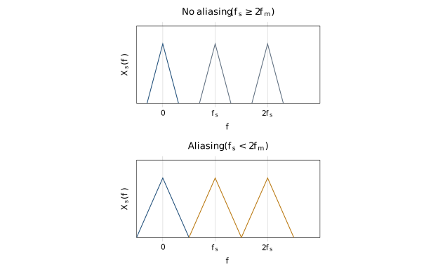
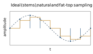
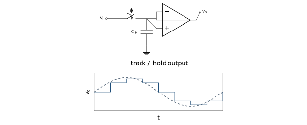
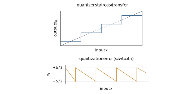
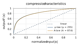
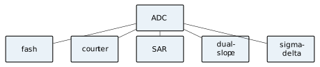
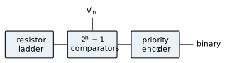
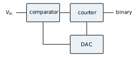
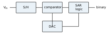
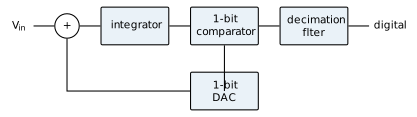
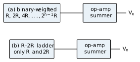
Fig: Analog-to-digital chain: anti-alias LPF, sample-and-hold, quantizer and encoder produce the digital outputFig: Digital-to-analog chain: the DAC converts each code to a level and a reconstruction LPF removes switching images and smooths the outputFig: Sampled spectra: separated replicas when f_s 2f_m (top) versus overlapping replicas that cause irreversible aliasing when f_s<2f_m (bottom)Fig: Sampling waveforms: dashed input, ideal impulse samples (stems), and a flat-top (held) staircase; natural sampling would gate the input with finite-width pulses whose tops follow the signalFig: Sample-and-hold: analog switch charges hold capacitor C_H during track, a high-impedance buffer isolates it during hold; the output tracks then holds each sampled valueFig: Uniform quantizer: staircase input-output characteristic (top) and the sawtooth error bounded by /2 (bottom)Fig: Companding chain: compressor and uniform quantizer/encoder at the transmitter; decoder and complementary expander at the receiverFig: -law and A-law compression curves: both enlarge low-level input spacing relative to the linear (dashed) responseFig: Taxonomy of the five principal ADC architecturesFig: Flash ADC: resistor ladder and a bank of parallel comparators feed a priority encoderFig: Counter ADC: a counter drives a DAC whose output is compared with V_in in a feedback loopFig: SAR ADC: comparator, feedback DAC and successive-approximation register run an MSB-to-LSB binary search on the held inputFig: Dual-slope ADC: integrator, zero comparator and control/counter integrate up on V_in then down on V_refFig: First-order sigma-delta ADC: summing node, integrator, 1-bit quantizer, 1-bit DAC feedback and a digital decimation filterFig: DAC structures: (a) binary-weighted resistor network and (b) R-2R ladder, each summed by an op-amp