Communication Circuits
Possible Exam Questions
Exam Questions and Answer Map
Evidence note: [PYQ paper/year] = exact question observed in that past paper; [likely] = pattern-predicted variant not confirmed as an exact PYQ.
- Explain low-level and high-level AM generation. Compare their power-amplifier requirements. [5] — [likely]
- Answer plan: Draw both signal paths -> low-level modulation before RF amplification requires linear following stages -> high-level modulation varies final Class-C stage supply and needs AF power -> compare efficiency, power and complexity.
-
Model answer: Low-Level and High-Level AM Generation
-
Explain a balanced modulator and diode-ring modulator. Why is the carrier suppressed? [10] — [likely]
- Answer plan: State product relation \(v_o=Km(t)c(t)\) -> explain symmetry cancellation -> draw balanced block and four-diode ring -> describe alternate carrier switching of diode pairs -> list isolation, DSB-SC output and practical imbalance.
-
Model answer: Balanced and Diode-Ring Modulators
-
Draw and explain an AM envelope detector. Derive the RC condition and explain diagonal and negative-peak clipping. [10] — [likely]
- Answer plan: Draw diode with parallel \(RC\) load -> explain peak charging and discharge -> state \(1/f_c\ll RC\ll1/f_m\) and modulation-dependent limit -> identify small-\(RC\) ripple, large-\(RC\) diagonal clipping, overmodulation and AC-loading distortion.
-
Model answer: AM Envelope Detector and Distortion
-
Explain coherent/product detection of DSB-SC and SSB. What are the effects of carrier phase and frequency error? [10] — [likely]
- Answer plan: Draw multiplier + recovered carrier + LPF -> derive baseband term -> show \(\cos\phi\) attenuation and beat from \(\Delta\omega\) -> state PLL/Costas/squaring recovery and SSB BFO requirement.
-
Model answer: Product Detection and Carrier Errors
-
Compare slope, Foster-Seeley, ratio and PLL FM detectors. Why is a limiter required? [10] — [likely]
- Answer plan: Begin with discriminator S-curve -> slope converts FM to AM -> Foster-Seeley phase imbalance needs limiter -> ratio detector holds voltage sum and rejects AM -> PLL control voltage tracks frequency -> compare linearity and circuit requirements.
-
Model answer: Slope, Foster-Seeley, Ratio and PLL FM Detectors
-
Explain the generation and detection circuits for ASK, BFSK, BPSK and QPSK. [10] — [likely]
- Answer plan: Use switch/product/VCO/IQ blocks -> distinguish coherent and noncoherent receivers -> show correlator/filter decisions -> state carrier and clock recovery requirements.
- Model answer: ASK, BFSK, BPSK and QPSK Circuits
1. Circuit Selection Map
Communication theory defines a waveform; a communication circuit must create or recover it with practical devices, biasing, filtering and synchronization.
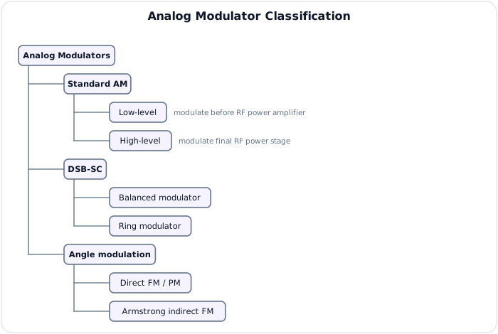
| Required waveform | Common generator | Common detector |
|---|---|---|
| Standard AM | Low-level multiplier or high-level collector/drain modulator | Diode envelope detector |
| DSB-SC | Balanced/product or ring modulator | Coherent product detector |
| SSB-SC | DSB-SC + filter, or phase-shift network | Product detector + BFO/carrier recovery |
| FM | VCO/reactance modulator or Armstrong method | Discriminator, ratio detector or PLL |
| PM | Phase modulator | Phase detector/PLL, or discriminator + integrator |
| ASK/OOK | Carrier switch/product modulator | Envelope or coherent detector |
| BFSK | VCO/two oscillators | Filter-energy detector, discriminator or correlators |
| BPSK/QPSK/QAM | Balanced I/Q product modulators | Coherent I/Q correlator receiver |
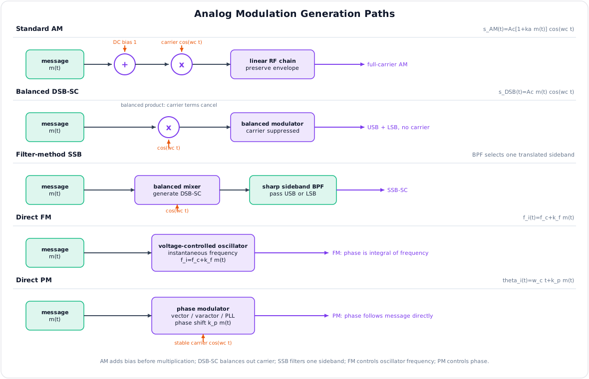
The exact transistor/op-amp implementation can vary; the exam should emphasize the signal operation and required transfer characteristic.
2. Standard AM Modulators
The required standard-AM output is:
For distortion-free envelope detection, \(|k_am(t)|\leq1\).
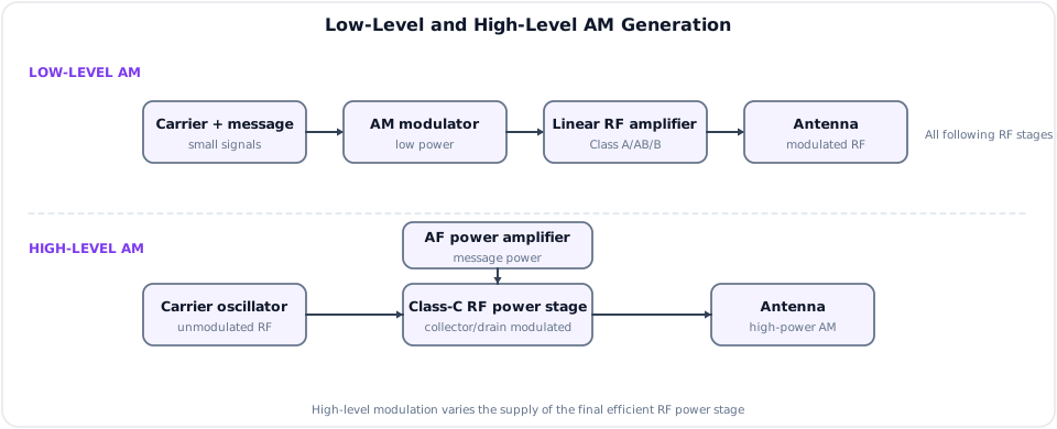
Low-Level and High-Level Paths
Low-Level Modulator
The message and carrier are combined at low power. The resulting AM waveform is amplified to transmitter output power.
Circuit methods:
- Diode or transistor square-law modulator.
- Four-quadrant analog multiplier.
- Variable-gain amplifier controlled by the message.
Key requirement: every RF stage after modulation must preserve the envelope, so linear Class A, AB or B amplification is used. Linear operation lowers transmitter efficiency at high power.
High-Level Modulator
The unmodulated carrier is amplified by an efficient nonlinear RF power stage, commonly Class C, and the audio signal varies its collector/drain supply or another final-stage parameter.
For ideal 100% sinusoidal modulation, the modulating audio stage must supply a substantial fraction of carrier power. In a classic plate/collector-modulated transmitter, peak audio power requirement reaches approximately half the unmodulated carrier input/output power under idealized assumptions.
Advantages: high RF efficiency and suitability for high transmitter power.
Limitations: needs a high-power audio amplifier and modulation transformer or equivalent supply modulator.
Comparison
| Feature | Low-level AM | High-level AM |
|---|---|---|
| Modulation point | Before RF power amplification | At final RF power stage |
| Message power | Small | High |
| Following RF stages | Must be linear | Final stage may be Class C/switching |
| Overall efficiency | Lower | Higher |
| Main use | Low/medium power, integrated transmitters | High-power broadcast transmitters |
3. DSB-SC Modulators
Balanced Product Modulator
An ideal product modulator multiplies message and carrier:
For \(m(t)=A_m\cos\omega_mt\):
There is no standalone carrier term.
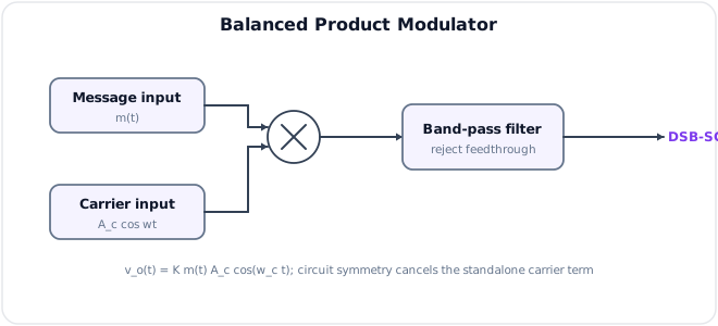
Practical realizations use matched diodes, a differential pair, Gilbert-cell multiplier or two amplitude modulators in push-pull. Symmetry causes equal carrier feedthrough terms to cancel while the cross-product terms add.
Practical limitations: device mismatch, transformer imbalance and DC offsets leave a residual carrier. Carrier suppression is specified in decibels relative to a sideband or unsuppressed carrier.
Diode-Ring (Double-Balanced) Modulator
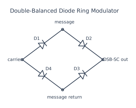
A strong carrier alternately forward-biases opposite diode pairs. The ring reverses the polarity of the message at the carrier rate, approximating multiplication by a square wave. A bandpass filter selects the desired DSB-SC components around \(f_c\).
Double-balanced behavior:
- Carrier feedthrough cancels at the output by symmetry.
- Message/baseband feedthrough also cancels.
- Output includes sum/difference products and higher odd switching products; filtering is required.
- Diodes need no DC bias in a passive ring and can handle a wide dynamic range.
The same topology is widely used as a passive mixer.
4. SSB Generation Circuits
Filter Method
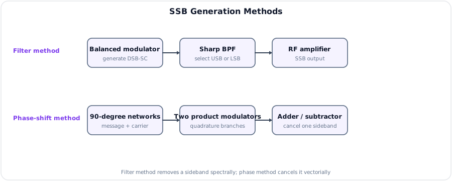
- A balanced modulator generates DSB-SC.
- A sharp bandpass filter passes only USB or LSB.
- Linear RF stages amplify the selected sideband.
Challenge: for low message frequencies, the two sidebands lie very close near \(f_c\), requiring a highly selective crystal/mechanical filter or generation at a convenient IF followed by mixing.
Phase-Shift Method
Create \(90^\circ\) phase-shifted versions of both message and carrier. Two product modulators produce quadrature DSB-SC signals. Adding or subtracting the branch outputs cancels one sideband:
where \(\hat{m}(t)\) is the Hilbert-transform/\(90^\circ\) version of \(m(t)\).
Challenge: maintaining accurate \(90^\circ\) phase and equal amplitude over the complete message band.
Weaver Method
The Weaver method uses two stages of quadrature mixing with low-pass filtering, reducing the need for a wideband audio Hilbert network. It is common in DSP/software-defined implementations.
5. AM Demodulator Circuits
Envelope Detector
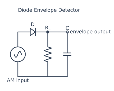
The diode conducts near positive carrier peaks and charges \(C\) rapidly to the envelope. Between peaks the diode is reverse-biased and \(C\) discharges through \(R_L\).
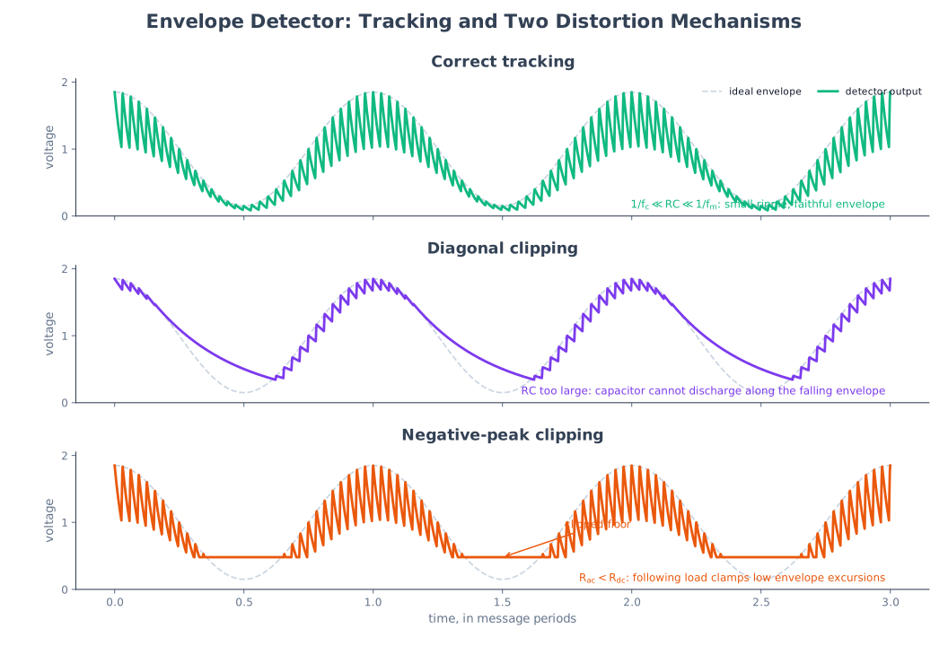
For the carrier ripple to be small and the fastest message variation to be followed:
For a single-tone standard-AM envelope, a more restrictive approximate no-diagonal-clipping condition is:
Detector Distortion
| Distortion | Cause | Remedy |
|---|---|---|
| Carrier ripple | \(RC\) too small | Increase time constant while retaining envelope tracking |
| Diagonal clipping | \(RC\) too large; capacitor cannot follow falling envelope | Reduce \(RC\) |
| Negative-peak clipping | AC load lower than DC load because following stage shunts \(R_L\) | Increase following-stage input impedance / isolate with buffer |
| Overmodulation distortion | \(\mu>1\), envelope crosses zero | Reduce transmitter modulation depth; envelope detector cannot repair it |
| Diode threshold distortion | Weak RF signal near diode drop | Bias/active detector or synchronous detection |
An envelope detector works for transmitted-carrier AM with a faithful envelope; it does not correctly recover ordinary DSB-SC or SSB.
Square-Law Detector
For a weak input, a nonlinear device may be approximated by:
The squared term contains a baseband component proportional to the message. An LPF removes RF terms. This method is useful for small signals but introduces higher-order distortion as input/modulation grows.
Product (Synchronous) Detector
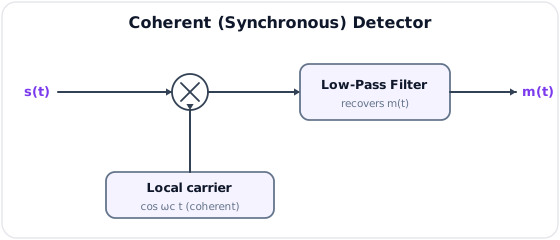
For DSB-SC \(s(t)=A_cm(t)\cos\omega_ct\) and local carrier \(2\cos(\omega_ct+\phi)\):
After low-pass filtering:
- Phase error \(\phi\) reduces output by \(\cos\phi\); at \(90^\circ\) the DSB-SC output is zero.
- Frequency error \(\Delta\omega\) produces a time-varying factor \(\cos(\Delta\omega t+\phi)\) and audible beat/fading.
- Carrier recovery uses a Costas loop, squaring loop or transmitted pilot.
- SSB uses a product detector with a BFO/reinserted carrier; frequency error shifts recovered speech frequencies.
6. FM Generation Circuits
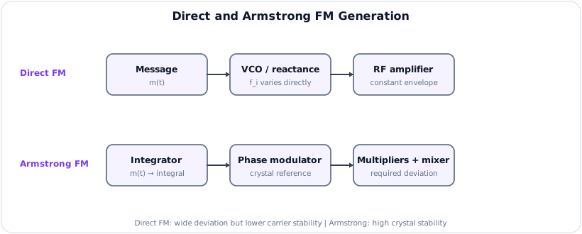
Direct FM
The message directly changes oscillator frequency:
Common methods:
- Apply message voltage to a varactor in an LC oscillator.
- Use a voltage-controlled oscillator.
- Use a reactance modulator whose effective capacitance/inductance varies with message.
Advantage: large deviation and simple generation.
Limitation: direct modulation of the oscillator can reduce carrier-frequency stability. A PLL can stabilize the long-term center frequency while allowing message-rate deviation.
Armstrong Indirect FM
- A crystal oscillator provides a stable carrier.
- Integrate \(m(t)\).
- Apply the integral to a phase modulator, producing narrowband FM.
- Use frequency multipliers to increase both carrier frequency and deviation.
- Mix to the desired final carrier band without changing deviation.
Advantage: excellent carrier stability.
Limitation: more stages and careful multiplier/mixer planning.
PM Generation
A phase modulator varies carrier phase directly:
It may use a varactor phase shifter, vector/IQ modulator or PLL phase-control path. FM is generated from PM by integrating the message first; PM is generated from FM by differentiating the message first.
7. FM Demodulator Circuits
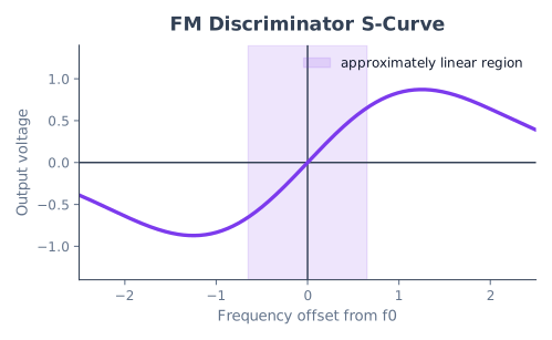
Every FM detector converts frequency deviation to voltage and ideally has a linear S-shaped transfer characteristic around \(f_c\).
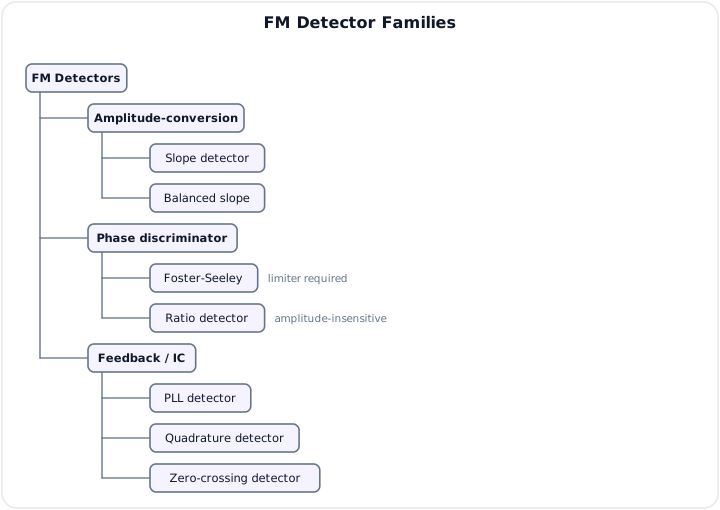
Slope Detector
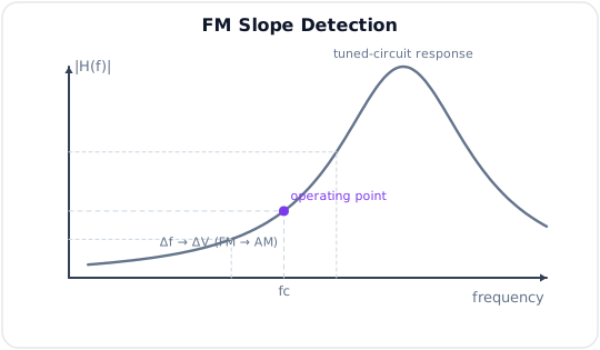
Place \(f_c\) on the approximately linear slope of a detuned resonant circuit. Frequency change produces amplitude change, then an envelope detector recovers the message.
Limitations: narrow linear range, poor symmetry and strong sensitivity to amplitude noise. A limiter is required before it.
Balanced Slope Detector
Two tuned circuits are centered on opposite sides of \(f_c\). Subtracting their rectified outputs gives a larger, more symmetric linear range and cancels some common amplitude variation. It still needs limiting.
Foster-Seeley Discriminator
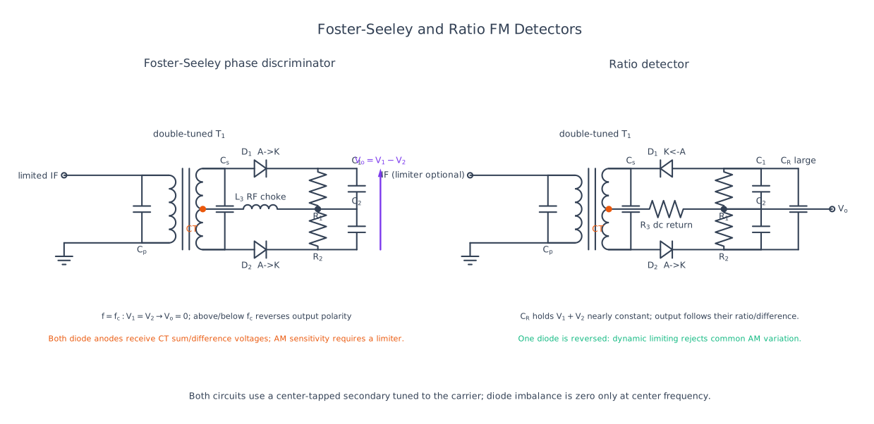
A center-tapped double-tuned transformer converts frequency deviation to a phase difference. Two diode rectifier outputs are equal at \(f_c\) and unequal above/below it; their difference is the message.
- Good linearity and output amplitude.
- Responds to amplitude variations, so a preceding limiter is required.
- Common in classical FM receivers.
Ratio Detector
The ratio detector uses a similar transformer but connects diodes and a large capacitor so the sum of diode voltages remains nearly constant. Output depends mainly on their ratio/difference.
- Substantial inherent rejection of amplitude changes.
- Usually no separate limiter required.
- Slightly lower output/linearity than a well-aligned Foster-Seeley circuit.
PLL FM Detector
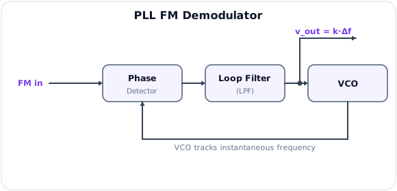
The PLL VCO tracks instantaneous input frequency. Within loop bandwidth and lock range:
Thus the loop-filter control voltage is the recovered message.
Advantages: excellent linearity, amplitude insensitivity, easy IC integration and no precision tuned discriminator transformer.
Design constraint: loop bandwidth must follow the highest message frequency and deviation dynamics while suppressing unwanted noise.
Quadrature Detector
Split limited FM into direct and frequency-dependent phase-shift paths. A multiplier/phase detector produces a voltage proportional to phase difference, hence frequency deviation near resonance. It is common in integrated FM receivers.
Detector Comparison
| Detector | Conversion principle | Limiter? | Linearity | Main feature |
|---|---|---|---|---|
| Slope | Detuned amplitude response | Yes | Poor | Simplest |
| Balanced slope | Difference of two slopes | Yes | Moderate | Symmetric response |
| Foster-Seeley | Transformer phase imbalance | Yes | Very good | High output |
| Ratio | Ratio of diode voltages | Usually no | Good | AM rejection |
| PLL | VCO control voltage tracks \(\Delta f\) | No separate limiter normally | Excellent in lock | IC-friendly |
| Quadrature | Frequency-dependent phase shift | Usually limited input | Good | IC-friendly |
8. Digital Modulator and Demodulator Circuits
ASK/OOK
Modulator: an RF switch controlled by unipolar data, or a product multiplier.
Noncoherent detector: RF/IF bandpass filter -> envelope detector -> LPF/matched filter -> clocked threshold.
Coherent detector: multiply by recovered carrier -> matched filter/integrator -> threshold.
BFSK
Modulator: binary-controlled VCO, direct digital synthesizer or switch between phase-continuous tones.
Noncoherent detector: two filters centered at \(f_0,f_1\) -> envelope/energy detectors -> compare.
Coherent detector: two synchronized correlators -> choose the larger metric.
Alternative: discriminator or PLL converts frequency to voltage, then a threshold recovers bits.
BPSK
Modulator: map bits to \(\pm1\) and drive a balanced product modulator.
Detector: Costas/carrier recovery -> product detector -> matched filter -> zero threshold. Differential encoding may resolve a \(180^\circ\) carrier-phase ambiguity.
QPSK and QAM
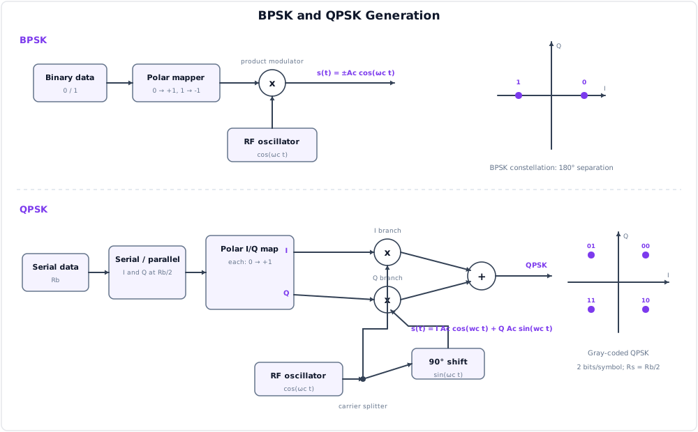
- Group serial bits and map them to I/Q amplitudes.
- Pulse-shape each branch.
- Multiply I by \(\cos\omega_ct\) and Q by \(-\sin\omega_ct\).
- Add branches and translate/amplify to RF.
- Receiver coherently downconverts to I/Q.
- Matched filters and symbol-timing recovery produce samples.
- A decision circuit selects the nearest constellation point.
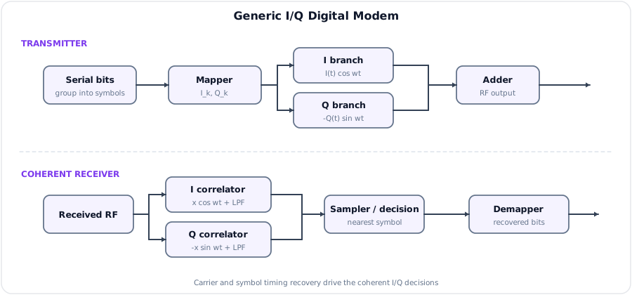
QAM amplitude variations require a linear transmitter chain or linearized PA. Constant-envelope FSK/MSK is more tolerant of saturated nonlinear PAs.
Essential Synchronizers
| Synchronizer | Function |
|---|---|
| Carrier recovery | Establish correct RF phase/frequency for coherent detection |
| Symbol timing recovery | Sample matched-filter output at optimum instant |
| Frame synchronization | Find word/packet boundaries |
| Automatic gain control | Scale I/Q samples to decision thresholds/constellation |
| Equalizer | Compensate amplitude/phase distortion and ISI |
9. Practical Circuit Metrics
| Metric | Why it matters |
|---|---|
| Carrier suppression | Residual carrier wastes power and can interfere with coherent schemes |
| Sideband suppression | Measures unwanted SSB/image rejection |
| Modulation error / EVM | RMS constellation error relative to ideal symbols |
| Frequency error | Causes rotation/beat and detector bias |
| Phase noise | Spreads carrier energy and degrades high-order QAM |
| Linearity / IP3 | Limits intermodulation and spectral regrowth |
| PAPR | Determines PA back-off for QAM/OFDM-like waveforms |
| Conversion gain/loss | Relates input and output power through mixer/modulator |
| Port isolation | Prevents LO, RF or message feedthrough |
Exam circuit answers should always label input, output, carrier/LO, filters and feedback paths, then explain which unwanted terms are rejected.
10. Key Exam Points
Key Exam Points - Communication Circuits
- Low-level AM needs linear RF amplification after modulation; high-level AM modulates the efficient final RF power stage.
- Balanced and ring modulators use symmetry to suppress carrier and produce DSB-SC.
- SSB is generated by filtering one DSB-SC sideband or by quadrature phase cancellation.
- Envelope detector condition: \(1/f_c\ll RC\ll1/f_m\); large \(RC\) causes diagonal clipping.
- DSB-SC and SSB require a product detector and synchronized/reinserted carrier.
- Direct FM varies an oscillator; Armstrong FM uses a stable phase modulator plus multipliers/mixers.
- Foster-Seeley needs a limiter; the ratio detector has inherent AM rejection; PLL output is its control voltage.
- ASK can use envelope detection, BFSK can use energy detection, while BPSK/QPSK/QAM normally use coherent correlators.
Model Answer - Low-Level and High-Level AM Generation [5 marks]
Exam-ready answer
Standard AM requires
with \(|k_am(t)|\leq1\) for a nonreversing envelope. The two transmitter methods differ mainly in where this waveform is formed and therefore in power-amplifier class.
In low-level modulation, a diode/transistor square-law circuit, analog multiplier or variable-gain amplifier combines message and carrier at small power. Buffer, driver and final RF stages then raise the already modulated signal to antenna power. Every following RF stage must preserve amplitude, so Class A, AB or B linear amplification and suitable back-off are required. The message amplifier is low power and the circuit is easy to control, but linear RF efficiency is limited and nonlinearity causes envelope distortion/spectral regrowth.
In high-level modulation, the unmodulated carrier is first amplified by an efficient Class-C or switching RF final stage. A high-power audio amplifier varies its collector/drain supply or another final-stage parameter, creating AM at output power. This gives high RF efficiency and suits broadcast transmitters, but needs a modulation transformer or supply modulator and substantial audio power; for ideal \(100\%\) sinusoidal plate/collector modulation, peak audio power capability is approximately \(P_c/2\) under the classical assumptions.
Thus low-level AM uses little audio power but requires linear RF power gain after modulation; high-level AM permits an efficient nonlinear RF final stage but transfers the power burden to the audio modulator. For a \(1\,\text{kW}\) carrier at \(\mu=1\), total RF power is \(1.5\,\text{kW}\) and sidebands total \(0.5\,\text{kW}\), consistent with the approximate high-level audio requirement. Low-level is common in low/medium-power integrated transmitters; high-level is favored at high broadcast power.
Practice target: 7-8 minutes; draw both paths and make the PA-linearity versus audio-power trade-off explicit.
Model Answer - Balanced and Diode-Ring Modulators [10 marks]
Exam-ready answer
A balanced or ring modulator generates DSB-SC by multiplying message and carrier while using symmetry to cancel direct feedthrough. For ideal multiplication,
If \(m(t)=A_m\cos\omega_mt\),
The output contains USB and LSB but no standalone \(\omega_c\) carrier term.
In a balanced modulator, matched diode/transistor branches receive the carrier with equal magnitude and opposite symmetry. Their carrier-only responses cancel at the output transformer/differential node, while the message-carrier cross-products have the polarity required to add. Implementations include push-pull modulators, differential pairs and Gilbert cells. A bandpass filter passes the DSB band and rejects harmonics. Device mismatch, bias offset and transformer imbalance cause residual carrier; carrier suppression is therefore a finite dB specification, not absolute in hardware.
In a diode-ring double-balanced modulator, a strong LO alternately forward-biases opposite diode pairs. The message transformer's output polarity is reversed every half carrier cycle, approximating multiplication by a bipolar square wave. The fundamental square-wave component translates the message to \(f_c\pm f_m\); odd LO harmonics also create \(3f_c\pm f_m\), \(5f_c\pm f_m\), etc., so output filtering is essential. Double balance ideally cancels both carrier/LO feedthrough and baseband/RF feedthrough and gives useful port isolation. A passive ring needs no DC bias, tolerates large signals and has good linearity, but has conversion loss and requires adequate LO drive plus baluns/transformers.
For a \(5\,\text{kHz}\) tone and \(1\,\text{MHz}\) carrier, the wanted output components are \(995\) and \(1005\,\text{kHz}\); absence of a \(1000\,\text{kHz}\) line indicates ideal suppression. Compared with a single-balanced circuit, the ring suppresses both input feedthrough families and many even-order terms, but balance errors and diode capacitance reduce isolation at high frequency. The same ring topology is used as a mixer because multiplication produces controlled sum/difference translation. DSB-SC saves carrier power but keeps \(2B_m\) bandwidth and requires coherent detection.
Practice target: 16-18 minutes; derive the sidebands, explain branch cancellation and alternate diode-pair conduction, then list practical nonidealities.
Model Answer - AM Envelope Detector and Distortion [10 marks]
Exam-ready answer
An envelope detector recovers the message from standard transmitted-carrier AM using a diode followed by a parallel load resistor \(R_L\) and capacitor \(C\).
Near each positive carrier peak, the input exceeds capacitor voltage plus diode drop, the diode conducts and charges \(C\) rapidly to the new envelope. Between peaks the diode is reverse-biased and \(C\) discharges exponentially through \(R_L\):
The time constant must be long compared with a carrier period to suppress RF ripple but short compared with the fastest envelope variation:
as a cycle-based engineering rule. Using angular frequency, the corresponding lower scale is \(1/\omega_c\). For a sinusoidal AM envelope, the steepest falling slope gives the more restrictive approximate no-diagonal-clipping condition
If \(R_LC\) is too small, the capacitor discharges appreciably between carrier peaks, leaving carrier ripple at the output. If it is too large, the stored voltage cannot follow a rapidly falling envelope; the diode remains off and the exponential discharge cuts diagonally across the desired waveform, causing diagonal clipping. Negative-peak clipping occurs when the AC message load is lower than the DC detector load, often because the following amplifier/coupling network shunts \(R_L\); the negative envelope requires more discharge than the circuit permits. A high-input-impedance buffer or correctly designed coupling removes this unequal loading. For \(\mu>1\), the transmitted envelope itself crosses zero, so no RC choice can prevent overmodulation distortion. Diode threshold also distorts weak signals; biased/active or synchronous detectors improve low-level operation.
For \(f_c=1\,\text{MHz}\), \(f_m=5\,\text{kHz}\) and \(\mu=0.8\), the modulation-dependent upper bound is
The carrier angular-time scale is \(1/(2\pi f_c)=0.159\,\mu\text{s}\), so a value around \(5\)-\(10\,\mu\text{s}\) is plausible after accounting for diode/source/load details. For \(R_L=10\,\text{k}\Omega\), \(C=1\,\text{nF}\) gives \(10\,\mu\text{s}\). Envelope detection is simple and needs no local oscillator, but works only when a transmitted carrier creates a faithful envelope; ordinary DSB-SC and SSB require coherent detection.
Practice target: 16-18 minutes; draw charge/discharge current paths, derive both RC inequalities, and distinguish ripple, diagonal, negative-peak and overmodulation distortion.
Model Answer - Product Detection and Carrier Errors [10 marks]
Exam-ready answer
A product or synchronous detector multiplies a suppressed-carrier input by a locally reconstructed carrier and low-pass filters the result. It preserves the signed message and is therefore used for DSB-SC and SSB.
For DSB-SC
and local oscillator \(2\cos[(\omega_c+\Delta\omega)t+\phi]\), multiplication gives sum and difference terms. After the LPF removes the component near \(2\omega_c\),
With exact frequency, \(\Delta\omega=0\), the recovered output is \(A_cm(t)\cos\phi\). A phase error therefore attenuates and possibly inverts the output: \(\phi=0^\circ\) gives maximum, \(90^\circ\) gives zero, and \(180^\circ\) gives inverted message. At \(30^\circ\), amplitude is \(\cos30^\circ=0.866\) of ideal. Frequency error makes the multiplier vary with time and produces periodic fading/beating; even a small offset prevents stationary recovery.
For SSB, a BFO/PLL carrier translates the one RF sideband back to its original baseband. A carrier-frequency error does not merely cause a common fade: it shifts every recovered audio frequency by \(\Delta f\), changing speech pitch and intelligibility. Phase error rotates the recovered analytic signal and changes the mixture of message/Hilbert components. Accurate frequency is therefore especially important in narrowband SSB voice; a \(20\,\text{Hz}\) BFO error shifts a \(1\,\text{kHz}\) tone to approximately \(980\) or \(1020\,\text{Hz}\) depending on sideband/injection.
Carrier recovery methods are a transmitted pilot/residual carrier, squaring loop for suitable suppressed-carrier waveforms, Costas loop for DSB/PSK, or a manually/automatically controlled BFO for SSB. The LPF bandwidth must pass the full message but reject the doubled-carrier product. Gain/phase imbalance, LO leakage, DC offset and finite carrier-recovery bandwidth are practical limitations. Unlike an envelope detector, which yields \(|m(t)|\) and loses DSB phase reversals, coherent detection recovers polarity and can demodulate weak suppressed-carrier signals, at the cost of synchronization circuitry.
Practice target: 16-18 minutes; derive the LPF output with both \(\phi\) and \(\Delta\omega\), then separately explain DSB fading and SSB frequency translation.
Model Answer - Slope, Foster-Seeley, Ratio and PLL FM Detectors [10 marks]
Exam-ready answer
An FM detector converts instantaneous frequency deviation into voltage. Around center frequency \(f_c\), its desired S-curve is
where \(K_D\) is detector sensitivity in volts per hertz. Output is zero at \(f_c\) and has opposite polarities above and below it.
A slope detector tunes a resonant circuit so \(f_c\) lies on one amplitude-response slope. Frequency movement becomes amplitude movement and a diode envelope detector recovers the message. It is simplest but has narrow linear range, asymmetric distortion and strong AM/noise sensitivity. A limiter is required. A balanced slope detector subtracts two opposite slopes for better symmetry.
A Foster-Seeley discriminator uses a center-tapped double-tuned transformer. Frequency deviation changes secondary phase relative to the reference; two diode voltages are equal at \(f_c\) and unequal above/below, and their difference is audio. It gives high output and very good linearity but also responds to input amplitude, so a preceding limiter is essential.
A ratio detector uses a similar transformer with reversed diode/loading arrangement and a large capacitor that holds the sum of diode voltages nearly constant. Output depends mainly on their ratio/difference, giving inherent AM rejection. A separate limiter is normally unnecessary, although output and linearity may be lower than a well-aligned Foster-Seeley detector.
In a PLL detector, the phase detector and loop filter force the VCO to track input frequency. Within lock and loop bandwidth,
so loop-filter control voltage is the recovered message. It has excellent linearity, strong amplitude immunity, wide design flexibility and easy IC integration, but must acquire/retain lock and its bandwidth must follow the highest message frequency without passing excessive noise.
The limiter removes parasitic amplitude changes before detectors whose output depends on RF amplitude; it preserves zero crossings and FM deviation. It is mandatory for slope and Foster-Seeley, largely built into the behavior of ratio detection, and usually not a separate requirement for a well-designed PLL input. For \(K_{VCO}=50\,\text{kHz/V}\) and \(\Delta f=25\,\text{kHz}\), PLL output peak is \(0.5\,\text{V}\). All detectors must cover peak deviation inside their linear/lock range; misalignment creates DC offset/distortion, and broadcast receivers add de-emphasis after detection.
Practice target: 16-18 minutes; sketch the S-curve, explain each conversion mechanism, and tabulate limiter need, linearity and main limitation.
Model Answer - ASK, BFSK, BPSK and QPSK Circuits [10 marks]
Exam-ready answer
Digital modulators map bits to controlled carrier waveforms; receivers filter/correlate the noisy waveform, recover timing/carrier where necessary and decide the most likely symbol.
ASK/OOK: a unipolar bit \(b(t)\in\{0,1\}\) controls an RF switch or multiplier, giving \(s(t)=A_cb(t)\cos\omega_ct\). A noncoherent receiver uses BPF \(\rightarrow\) envelope detector \(\rightarrow\) matched/low-pass filter \(\rightarrow\) clocked threshold. Coherent ASK instead multiplies by a recovered carrier and integrates/correlates. OOK is simple but amplitude noise/fading directly moves its decision metric.
BFSK: bits select two tones \(f_0\) and \(f_1\) using a VCO, DDS or phase-continuous oscillator switch. A noncoherent receiver has two bandpass filters and energy/envelope detectors; it chooses the larger energy. A coherent receiver uses two synchronized correlators, while a discriminator or PLL may convert mark/space frequency to two voltages. BFSK tolerates nonlinear PAs and amplitude variation but generally uses more bandwidth than PSK.
BPSK: map bits to \(a_k=\pm1\) and drive a balanced product modulator, so carrier phase is \(0\) or \(\pi\). The coherent receiver uses carrier recovery/Costas loop \(\rightarrow\) product detector \(\rightarrow\) matched filter or integrate-and-dump \(\rightarrow\) zero-threshold decision. Differential encoding can remove the \(180^\circ\) carrier-phase ambiguity. BPSK has strong power efficiency but requires phase synchronization.
QPSK: a serial-to-parallel mapper forms I and Q symbols in \(\{\pm1\}\). Pulse-shaped branches multiply orthogonal carriers and add:
At the receiver, coherent quadrature LOs down-convert to I/Q, matched filters maximize sampled SNR, symbol-timing recovery chooses sample instants, and two sign decisions recover two bits per symbol. Gray mapping limits most nearest-neighbor errors to one bit.
Carrier recovery is essential for BPSK/QPSK; symbol timing is essential for all four, and frame/AGC/equalization may also be required. For \(R_s=1\,\text{Msymbol/s}\), BPSK carries \(1\,\text{Mbit/s}\) while QPSK carries \(2\,\text{Mbit/s}\) before coding, explaining QPSK's bandwidth efficiency. Practical filters limit occupied spectrum but introduce ISI unless matched/equalized; frequency/phase error rotates PSK decisions, while nonlinear PA operation distorts amplitude-varying signals. ASK favors simplicity, BFSK robustness/noncoherent options, BPSK power efficiency and QPSK twice the bits per symbol.
Practice target: 17-19 minutes; draw each modulator/detector path, distinguish coherent from noncoherent detection, and state all synchronization needs.