Differential and Cascode Amplifiers
Possible Exam Questions
Exam Questions and Answer Map
-
Draw a BJT differential amplifier, explain its operation, and derive differential gain, common-mode gain and CMRR. [10] — [likely]
-
Answer plan: Define the differential pair → draw the matched circuit → explain balanced, differential and common-mode operation → derive \(A_d\), \(A_c\) and CMRR → state applications.
-
Model answer: BJT Differential Amplifier and CMRR
-
Why is a constant-current source or current mirror used in the tail of a differential amplifier? [5] — [likely]
-
Answer plan: Identify the tail path → show that a current source has high small-signal resistance → relate lower common-mode gain to higher CMRR → compare resistor, Zener source and mirror.
-
Model answer: Constant-Current Tail and Current Mirror
-
Draw and explain BJT and FET cascode amplifiers. Why does a cascode have wide bandwidth? [5] — [likely]
-
Answer plan: Draw CE–CB and CS–CG stacks → trace signal current → explain nearly fixed collector/drain voltage → connect low Miller multiplication to larger bandwidth → list trade-offs and uses.
- Model answer: Cascode Amplifier and Miller-Effect Reduction
High-Scoring Answer Pattern
| Marks | What the examiner should see |
|---|---|
| 1 | Exact definition and named configuration |
| 2 | Complete labelled circuit with supplies, inputs, output polarity and tail/bias network |
| 2 | Physical operation for balanced and signal conditions |
| 3 | Assumptions, derivation steps and boxed result |
| 1 | Limitation or design trade-off |
| 1 | Two relevant applications |
Presentation Rule
Use one symbol consistently for the differential input, for example \(v_{id}=v_1-v_2\), and define the output polarity before writing gain. This prevents a correct derivation from losing marks because of an unexplained sign or factor of two.
1. Differential Amplifier
Definition
A differential amplifier is a direct-coupled amplifier that:
- has two input terminals, \(v_1\) and \(v_2\);
- amplifies their difference \(v_{id}=v_1-v_2\);
- rejects the component common to both inputs;
- commonly forms the input stage of an op-amp.
The input decomposition is
Basic BJT Circuit
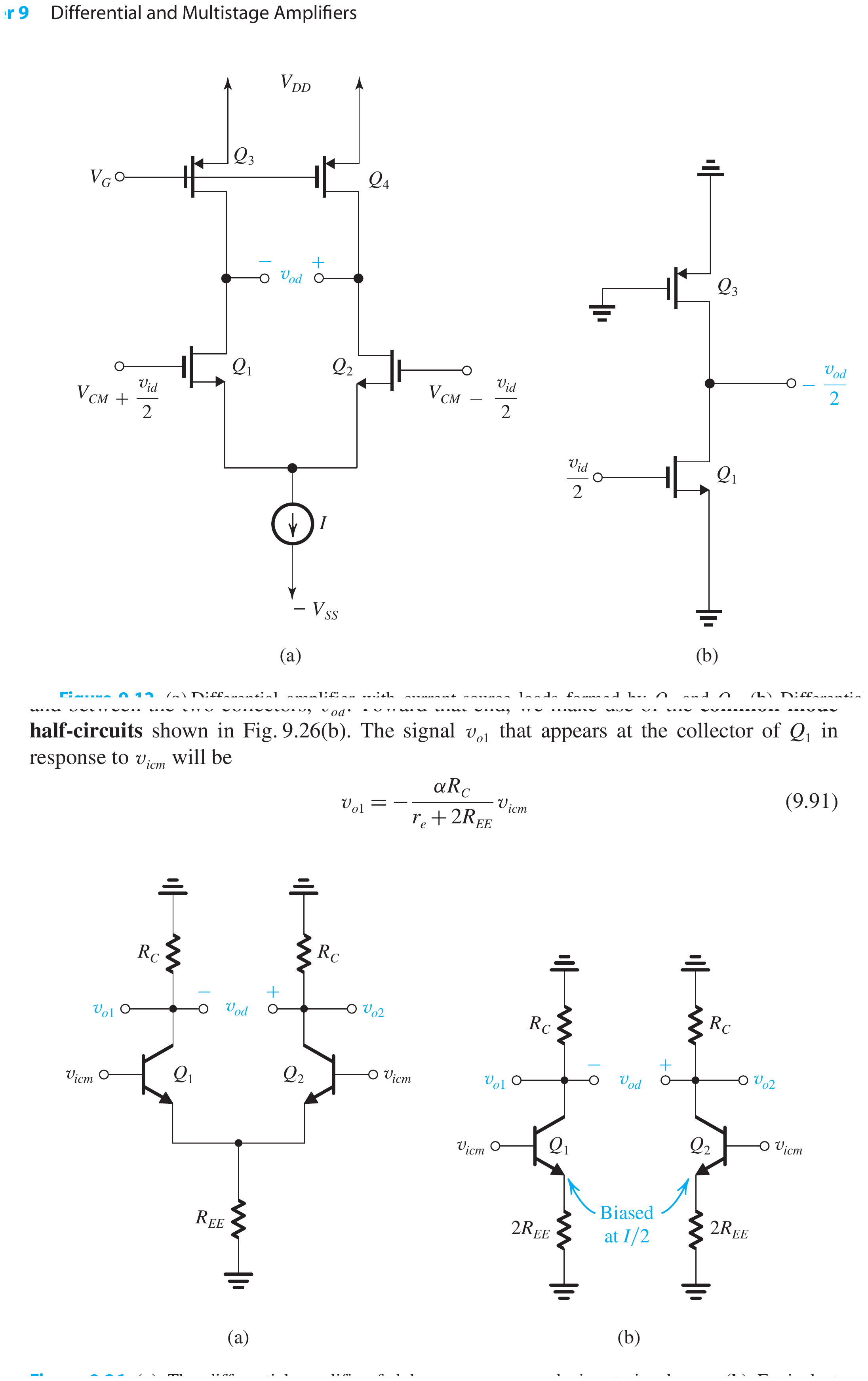
Parts and Functions
| Part | Function |
|---|---|
| Matched \(Q_1,Q_2\) | Convert differential base voltage into complementary collector-current changes |
| Equal \(R_C\) | Convert collector-current changes into output voltages |
| Shared \(R_E\) | Establish tail current and oppose common-mode current change |
| \(+V_{CC},-V_{EE}\) | Permit bipolar signal swing and direct coupling around \(0\) V |
| Two collector nodes | Provide single-ended or double-ended output |
Quiescent Balanced Condition
For matched transistors with \(v_1=v_2\):
- \(V_{BE1}=V_{BE2}\);
- tail current divides equally;
- \(I_{C1}\approx I_{C2}\approx I_T/2\);
- collector drops are equal;
- differential output \(v_{od}=v_{c2}-v_{c1}=0\) ideally.
Mismatch, temperature gradient and input offsets produce a small practical output offset.
Differential-Mode Operation
Let
For a positive \(v_{id}\):
- \(V_{BE1}\) rises and \(i_{c1}\) increases.
- \(V_{BE2}\) falls and \(i_{c2}\) decreases.
- The drop across the left \(R_C\) increases, so \(v_{c1}\) falls.
- The drop across the right \(R_C\) decreases, so \(v_{c2}\) rises.
- The collector outputs therefore move in opposite directions.
The pair steers an almost constant tail current between the two collector branches.
Common-Mode Operation
For a common-mode signal,
- Both transistor currents try to change in the same direction.
- Their sum changes the voltage across the common tail element.
- Tail degeneration raises both emitter voltages and opposes the input change.
- Equal collector changes cancel in an ideal double-ended output.
- Device/load mismatch leaves a finite practical common-mode output.
2. Differential Gain, Common-Mode Gain and CMRR
Assumptions for the Short Derivation
- \(Q_1,Q_2\) and \(R_C\) are matched.
- Transistor output resistance is large.
- \(\beta\) is large, so emitter and collector current changes are approximately equal.
- \(r_e'\) is the small-signal emitter resistance.
This approximation applies at room temperature.
Differential-Mode Gain
Each emitter receives half the differential input in magnitude:
Therefore
For \(v_{od}=v_{c2}-v_{c1}\),
At one collector,
Here de means double-ended output and se means single-ended output.
Common-Mode Gain
Both emitter-current increments pass through \(R_E\). Each transistor therefore experiences strong common emitter degeneration:
Thus a larger effective tail resistance gives a smaller common-mode gain.
Common-Mode Rejection Ratio
In general,
Using the convention common in the prescribed text, \(A_d=R_C/r_e'\) and \(A_c=R_C/(2R_E)\):
Gain-Convention Trap
A double-ended differential output ideally cancels common mode, whereas a single collector has finite \(A_c\). If both gains are defined at one collector, \(|A_{d,se}/A_{c,se}|\approx R_E/r_e'\). If the question or text uses \(A_d=R_C/r_e'\), it is using the double-ended differential-gain convention and usually expects \(2R_E/r_e'\). State the convention and follow it consistently.
Why High CMRR Matters
High CMRR allows the amplifier to reject:
- mains hum induced equally in both leads;
- electromagnetic pickup on a balanced cable;
- sensor lead interference;
- ground-potential variation;
- supply- or temperature-related common drift.
3. Improving CMRR with an Active Tail
The tail resistor improves rejection only by being large, but a very large physical resistor needs excessive DC voltage. An active current source provides:
- the required DC tail current;
- very high small-signal output resistance;
- better CMRR without impractical supply voltage;
- improved bias stability.
Zener-Referenced Constant-Current Sink
Operation:
- \(R_2\) biases the Zener diode.
- The Zener fixes the base voltage of \(Q_3\) relative to \(-V_{EE}\).
- The emitter voltage is approximately one \(V_{BE}\) below the base voltage.
- \(R_1\) therefore sets an almost constant current.
- Common-mode input change produces little tail-current change because the collector output resistance of \(Q_3\) is high.
Practical limits:
- Zener noise enters the tail current;
- \(V_Z\) and \(V_{BE}\) drift with temperature;
- \(Q_3\) needs compliance voltage to remain active;
- finite transistor output resistance makes CMRR finite.
Current-Mirror Tail
Operation:
- \(Q_4\) is diode-connected, so its collector and base establish \(V_{BE}\).
- \(R\) sets reference current \(I_{ref}\).
- Matched \(Q_3\) receives nearly the same \(V_{BE}\) and mirrors the current.
- For the shown dual-supply connection, the reference and tail currents are approximately:
- The mirror behaves as a high-resistance current sink at the common emitters.
Accuracy is limited by transistor mismatch, finite \(\beta\), Early effect, temperature difference and unequal collector voltages.
Tail Comparison
| Tail element | DC-current control | Small-signal resistance | CMRR | Main limitation |
|---|---|---|---|---|
| Resistor \(R_E\) | Supply and resistor | \(R_E\) | Moderate | Large resistance needs large voltage |
| Zener current sink | \(V_Z,R_1\) | High | High | Zener noise and temperature drift |
| Current mirror | Reference branch and matching | High | High | Matching, compliance and finite \(\beta\) |
4. Practical Differential-Pair Errors
Input Offset Voltage
- Small differential input required to force \(v_o=0\).
- Caused by \(V_{BE}\), \(R_C\) and geometry mismatch.
- Reduced by matched devices, symmetric layout and trimming.
Input Bias and Offset Currents
- Bias current produces drops in source resistances.
- Unequal source resistances convert bias current into differential error.
- Bias-current compensation uses approximately equal resistance seen by both bases.
Finite Output Range
- The input common-mode voltage must keep both input transistors active.
- The tail source needs minimum compliance voltage.
- Collector outputs need headroom above saturation.
- Excessive \(v_{id}\) steers nearly all tail current to one side and leaves the small-signal region.
5. Cascode Amplifier
Definition and Configurations
A cascode stacks a transconductance input stage below a current-buffer output stage:
- BJT cascode: common emitter (CE) followed by common base (CB);
- FET cascode: common source (CS) followed by common gate (CG).
It is one composite stage, not two ordinary voltage-gain stages connected through a coupling network.
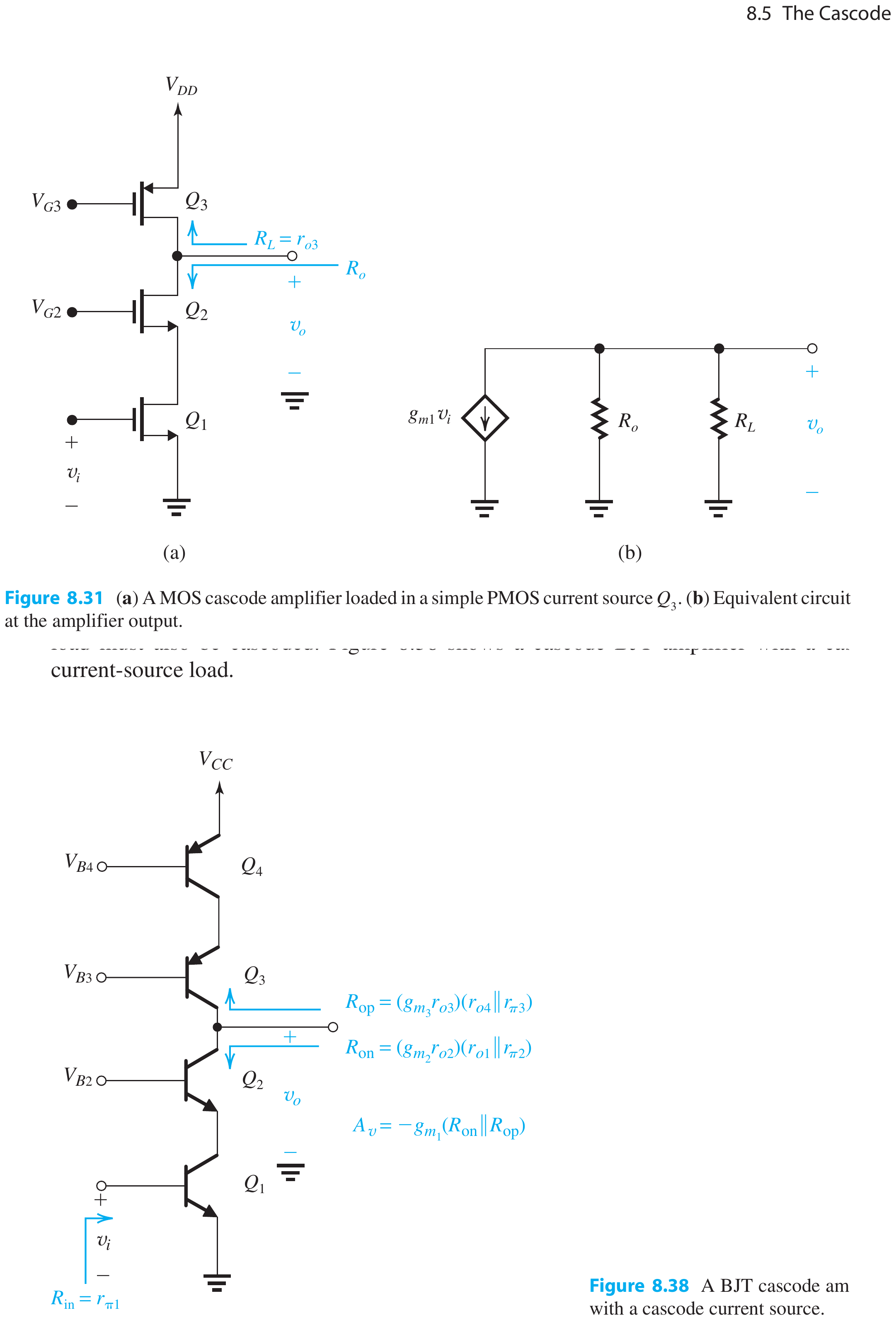
BJT Cascode Operation
- \(Q_1\) is the CE input transistor and converts \(v_i\) into collector-current variation.
- \(Q_2\) is biased in CB mode; \(C_B\) holds its base at AC ground.
- The emitter of \(Q_2\) presents low small-signal resistance to the collector of \(Q_1\).
- \(Q_1\) collector voltage therefore changes only slightly.
- \(Q_2\) transfers the signal current to \(R_C\).
- \(R_C\) converts the current variation into an amplified, inverted output voltage.
FET Cascode Operation
- \(Q_1\) is the CS input device and produces drain-current variation.
- \(Q_2\) is biased in CG mode; its gate is fixed for AC.
- The low impedance at the source of \(Q_2\) keeps the drain of \(Q_1\) nearly constant.
- \(Q_2\) conveys drain-current change to \(R_D\) and the output.
- Gate current remains approximately zero, giving very high input resistance.
Why the Miller Effect Is Suppressed
In an ordinary inverting stage, a feedback capacitance \(C_f\) between input and output appears at the input as
For large negative gain, \(C_{Mi}\approx C_f(1+|A_v|)\).
In the cascode:
- the collector/drain of the input device is held nearly at AC constant voltage;
- local voltage gain from its input to collector/drain is small;
- voltage change across \(C_{bc}\) or \(C_{gd}\) is small;
- Miller multiplication is therefore greatly reduced;
- input capacitance falls and the upper cutoff frequency rises.
Gain and Output Resistance
The input transistor supplies transconductance and the upper transistor supplies isolation and high output resistance. A useful estimate is
For a matched MOS cascode, the intrinsic output resistance is of order
when \(g_mr_o\gg1\). The exact gain is limited by the external collector/drain load and device parasitics.
Advantages
- much lower Miller multiplication;
- wider bandwidth and better high-frequency response;
- high reverse isolation from output to input;
- high output resistance and potentially high voltage gain;
- improved input-output isolation in RF stages.
Limitations
- two devices require more voltage headroom;
- output swing is smaller at low supply voltage;
- upper-device biasing adds components;
- extra device noise and mismatch remain;
- the high-output-resistance node can still have a limiting capacitance.
Applications
- RF and IF amplifiers;
- wideband oscilloscopes and measurement front ends;
- op-amp internal gain stages;
- low-noise amplifiers;
- current mirrors and active loads;
- high-gain integrated analog stages.
Cascode vs Cascade
| Feature | Cascode | Cascade |
|---|---|---|
| Connection | Devices stacked in one direct current path | Output of one complete stage drives another |
| Main purpose | Wide bandwidth, isolation, high output resistance | Multiply stage gains |
| Interstage voltage swing | Deliberately small | Usually significant |
| Miller effect in first device | Strongly reduced | May remain in each inverting stage |
| Headroom | Higher per composite stage | Distributed between separate stages |
Rapid Recall
- Differential pair: amplifies \(v_1-v_2\), rejects \(v_{cm}\).
- Positive \(v_1-v_2\): \(i_{C1}\) rises, \(v_{C1}\) falls; \(i_{C2}\) falls, \(v_{C2}\) rises.
- \(A_{d,de}\approx R_C/r_e'\).
- \(A_{c,se}\approx R_C/(2R_E)\).
- Prescribed convention: \(\text{CMRR}\approx2R_E/r_e'\).
- Active tail: high small-signal resistance → lower \(A_c\) → higher CMRR.
- Cascode: CE–CB or CS–CG.
- Nearly fixed collector/drain voltage → low Miller effect → wide bandwidth.
Model Answer — BJT Differential Amplifier and CMRR [10 marks]
Exam-ready answer
A BJT differential amplifier uses two matched transistors with equal collector loads and a common tail element. It amplifies \(v_{id}=v_1-v_2\) and rejects \(v_{cm}=(v_1+v_2)/2\).
At balance, \(v_1=v_2\), the tail current divides equally, collector voltages are equal and the double-ended output is zero. For positive \(v_{id}\), \(Q_1\) current rises and its collector voltage falls; \(Q_2\) current falls and its collector voltage rises. Thus the collector outputs are complementary.
With matched devices, large \(\beta\), transistor output resistance neglected and \(r_e'\approx26\,\text{mV}/I_E\),
Therefore, for \(v_{od}=v_{c2}-v_{c1}\),
With equal common-mode inputs, both currents try to change together. The shared \(R_E\) develops emitter feedback, giving the approximate single-collector common-mode gain
Under this prescribed gain convention,
A large effective tail resistance therefore improves common-mode rejection. A transistor current source or current mirror is preferred to an impractically large resistor. Applications include op-amp inputs, sensor bridges, balanced receivers and instrumentation.
Practice target: 18 minutes; define input/output polarities, draw the complete pair, derive both gains, box CMRR and state why an active tail improves it.
Model Answer — Constant-Current Tail and Current Mirror [5 marks]
Exam-ready answer
The tail element fixes the total emitter current of a differential pair. A resistor has finite small-signal resistance, so common-mode input changes alter tail current and produce common-mode gain. A transistor current source presents much higher small-signal resistance; hence \(A_c\) falls and CMRR rises.
In the Zener-referenced sink, the Zener fixes the base voltage of \(Q_3\) and \(R_1\) sets
In the mirror, diode-connected \(Q_4\) establishes \(V_{BE}\) from \(I_{ref}\) and matched \(Q_3\) sinks approximately the same current. The mirror is compact and suitable for IC fabrication. Its accuracy is limited by mismatch, finite \(\beta\), Early effect and compliance voltage.
Practice target: 8 minutes; draw either active tail, write its current equation and explicitly link high tail resistance to low \(A_c\) and high CMRR.
Model Answer — Cascode Amplifier and Miller-Effect Reduction [5 marks]
Exam-ready answer
A cascode combines a CE input transistor with a CB upper transistor, or a CS input FET with a CG upper FET.
The lower device converts input voltage into signal current. The upper CB/CG device transfers this current to the collector/drain load while presenting low impedance to the lower device's collector/drain. That node therefore has very small AC voltage swing.
Since the input device's feedback capacitance sees little voltage change, its Miller-equivalent input capacitance \(C_f(1-A_v)\) is not strongly multiplied. Input capacitance decreases, upper cutoff frequency rises and reverse isolation improves. The cascode also has high output resistance and useful voltage gain.
Advantages are wide bandwidth, low Miller effect, high output resistance and good input-output isolation. Limitations are extra biasing, more devices, greater voltage headroom and reduced output swing. Uses include RF/IF amplifiers, op-amp gain stages and wideband instrumentation.
Practice target: 8 minutes; label CE–CB or CS–CG and make “nearly fixed collector/drain voltage” the causal link between the circuit and wider bandwidth.