Logic Gates and Universal Gates¶
Possible Exam Questions¶
Exam Questions and Answer Map
Questions marked [PYQ paper/year] were directly observed in past papers; [likely] means pattern-based prediction, not a claimed past question. Rehearse each answer plan closed-book, then check the full answer via the links.
-
Draw the symbols and truth tables of the basic logic gates; why are NAND and NOR universal? [5] — [likely]
-
Answer plan: List AND, OR, NOT, NAND, NOR, XOR and XNOR → draw symbols/truth tables → realise NOT, AND and OR using one universal gate type.
- Model answer: Basic Logic Gates and Universal Gates
---dddddddd
Logic Gates — The Building Blocks of Logic Families¶
Likely Exam Question (5 marks)
"Draw the symbols and write the truth tables of the basic logic gates. Which gates are called universal gates and why?"
Before looking at how gates are built from transistors (TTL, NMOS and CMOS in the following sections), we fix the logic-level meaning of each gate — its symbol, Boolean expression and truth table. Throughout we use positive logic: HIGH = logic 1, LOW = logic 0.
The Seven Basic Gates¶
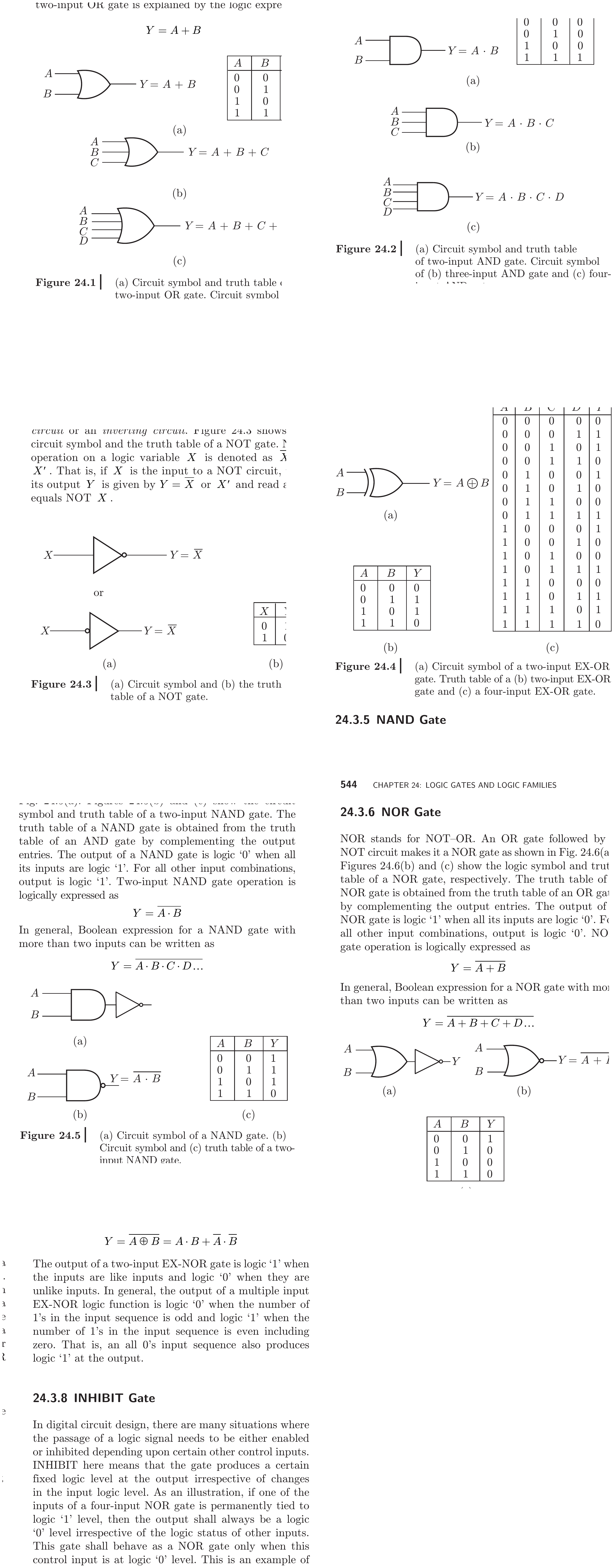
| Gate | Boolean expression | Output is 1 when… |
|---|---|---|
| AND | \(Y = A \cdot B\) | all inputs are 1 |
| OR | \(Y = A + B\) | any input is 1 |
| NOT (inverter) | \(Y = \overline{A}\) | the input is 0 |
| NAND | \(Y = \overline{A \cdot B}\) | any input is 0 (AND, then invert) |
| NOR | \(Y = \overline{A + B}\) | all inputs are 0 (OR, then invert) |
| XOR | \(Y = A \oplus B = A\overline{B} + \overline{A}B\) | the inputs are different |
| XNOR | \(Y = \overline{A \oplus B}\) | the inputs are the same (equality) |
Combined truth table (2-input gates):
| \(A\) | \(B\) | AND | OR | NAND | NOR | XOR | XNOR |
|---|---|---|---|---|---|---|---|
| 0 | 0 | 0 | 0 | 1 | 1 | 0 | 1 |
| 0 | 1 | 0 | 1 | 1 | 0 | 1 | 0 |
| 1 | 0 | 0 | 1 | 1 | 0 | 1 | 0 |
| 1 | 1 | 1 | 1 | 0 | 0 | 0 | 1 |
Universal Gates¶
NAND and NOR are called universal gates because any logic function can be implemented using only NAND gates (or only NOR gates). This matters for fabrication: a whole chip can be built by repeating a single gate type.
- NOT from NAND: tie both inputs together → \(\overline{A \cdot A} = \overline{A}\).
- AND from NAND: a NAND followed by a NAND-inverter → \(\overline{\overline{A\cdot B}} = A\cdot B\).
- OR from NAND: invert both inputs first → \(\overline{\overline{A}\cdot\overline{B}} = A + B\) (De Morgan).
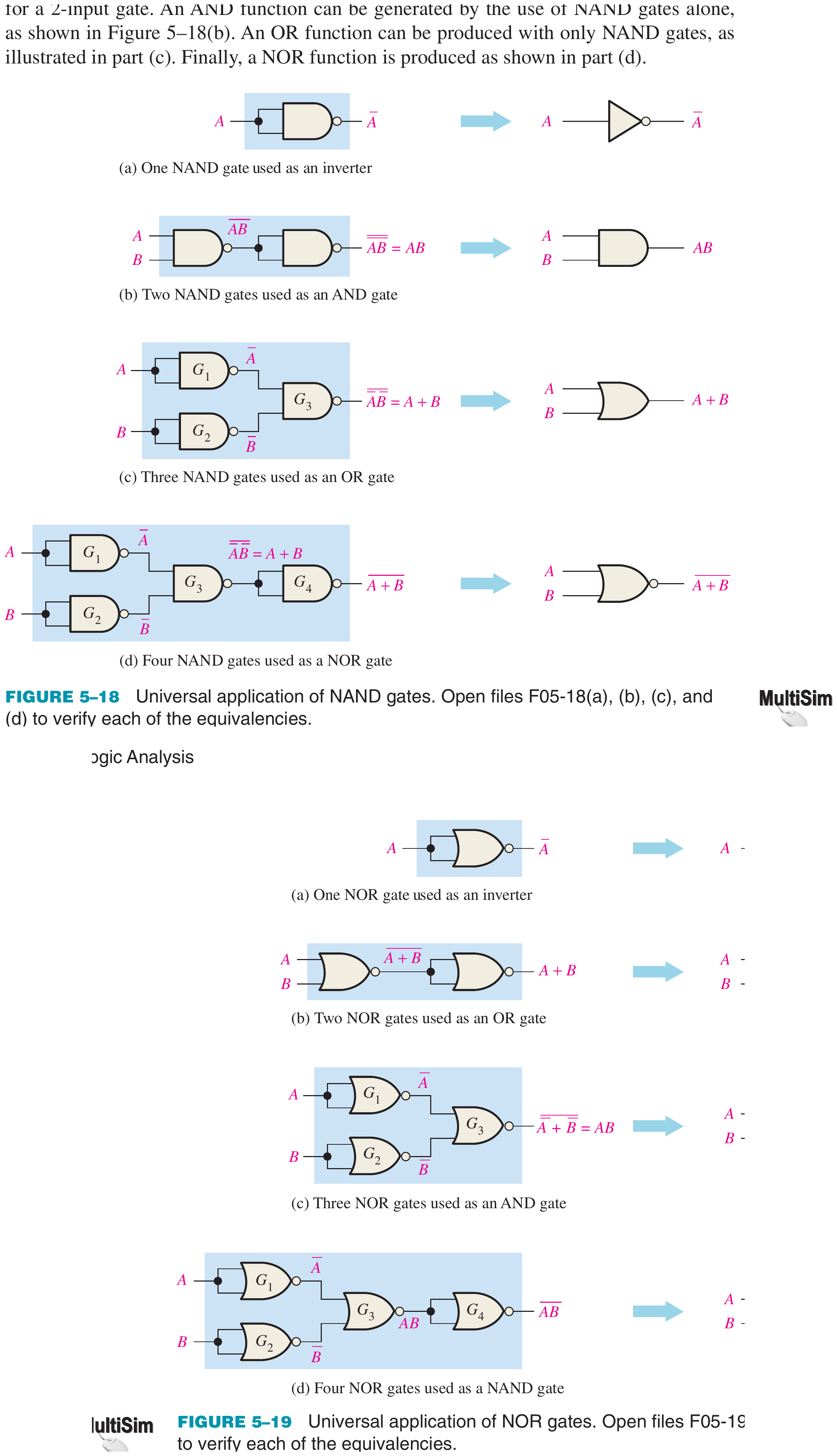
This "invert-then-combine" idea is exactly why CMOS and TTL naturally produce the inverting gates (NOT, NAND, NOR) and build AND/OR by adding an inverter — as the next two sections show.
Logic Families at a Glance¶
The same gate can be fabricated with different IC technologies (logic families). The chosen family fixes the gate's real-world characteristics — speed, voltage levels, noise margin, fan-out and power consumption. The common families, in order of historical appearance, are:
| Family | Full name | Built from | Status | Note |
|---|---|---|---|---|
| RTL | Resistor–Transistor Logic | resistors + BJTs | Obsolete | Earliest IC family; low fan-out, poor noise margin |
| DTL | Diode–Transistor Logic | diodes + BJTs | Obsolete | Diode AND-input; superseded by TTL |
| TTL | Transistor–Transistor Logic | BJTs (multi-emitter) | Legacy / in use | Fast and robust; the 7400 series (§2) |
| ECL | Emitter-Coupled Logic | BJTs (non-saturating) | In use | Fastest bipolar family — transistors never saturate, so there is no storage delay, but it draws high power |
| CMOS | Complementary MOS | NMOS + PMOS | Dominant | Near-zero static power; the VLSI workhorse (§5) |
RTL and DTL are now obsolete; modern design centres on TTL, ECL and CMOS. The next two sections build the gates of the two families named in the syllabus — TTL (bipolar) and NMOS/CMOS (unipolar).
Where this fits — circuit level vs logic level
This chapter treats gates at the transistor / circuit level — how each gate is physically realised in the TTL, NMOS and CMOS families (the EDC syllabus line “TTL logic circuits, NMOS/CMOS logic circuits”). The logic-level design built on top of these gates — Boolean algebra, K-map minimisation, adders, multiplexers, flip-flops and counters — lives in the separate Digital Logic chapters. Keep the two levels distinct: here = electronics of a gate; there = designing with gates.
Model Answer — Basic Logic Gates and Universal Gates [5 marks]¶
Exam-ready answer
A logic gate is a digital circuit that performs a Boolean operation on binary inputs, where 0 denotes LOW and 1 denotes HIGH in positive logic.
| \(A\) | \(B\) | AND \(AB\) | OR \(A+B\) | NAND \(\overline{AB}\) | NOR \(\overline{A+B}\) | XOR \(A\oplus B\) | XNOR \(\overline{A\oplus B}\) |
|---|---|---|---|---|---|---|---|
| 0 | 0 | 0 | 0 | 1 | 1 | 0 | 1 |
| 0 | 1 | 0 | 1 | 1 | 0 | 1 | 0 |
| 1 | 0 | 0 | 1 | 1 | 0 | 1 | 0 |
| 1 | 1 | 1 | 1 | 0 | 0 | 0 | 1 |
For a single input, NOT gives \(Y=\overline A\): \(0\mapsto1\) and \(1\mapsto0\). AND is 1 only when all inputs are 1; OR is 1 when any input is 1; XOR detects unequal inputs and XNOR detects equality.
NAND and NOR are universal because either gate alone can construct NOT, AND and OR, which form a functionally complete set.
Using NAND only:
Using NOR only:
The last identities follow from De Morgan's laws. Therefore any Boolean expression, and hence any combinational or sequential digital system, can be implemented using only NANDs or only NORs; this simplifies IC fabrication and spare-gate use.
Practice target: 8–9 minutes; draw the seven symbols, one combined truth table, and either universal-gate construction in full.